SNVS337F June 2006 – September 2015 LP38859
PRODUCTION DATA.
- 1 Features
- 2 Applications
- 3 Description
- 4 Revision History
- 5 Specifications
- 6 Detailed Description
- 7 Application and Implementation
- 8 Power Supply Recommendations
- 9 Layout
- 10Device and Documentation Support
- 11Mechanical, Packaging, and Orderable Information
封装选项
机械数据 (封装 | 引脚)
散热焊盘机械数据 (封装 | 引脚)
- KTT|5
订购信息
7 Application and Implementation
NOTE
Information in the following applications sections is not part of the TI component specification, and TI does not warrant its accuracy or completeness. TI’s customers are responsible for determining suitability of components for their purposes. Customers should validate and test their design implementation to confirm system functionality.
7.1 Application Information
The LP38859 can provide 3-A output current with 240-mV dropout voltage (typical). The bias voltage must be in the range of 3 V to 5.5 V to ensure proper operation of the device. The input voltage must be at least VOUT + VDO, and no higher than whatever value is used for VBIAS. Minimal input and output capacitors are each 10 μF. The capacitor on the BIAS pin must be at least 1 μF.
7.2 Typical Application
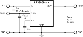 Figure 20. LP38859 Typical Application
7.2.1 Design Requirements
For typical high-accuracy LDO linear regulator applications, use the parameters listed in Table 1.
Table 1. Design Parameters
| DESIGN PARAMETER | EXAMPLE VALUE |
|---|---|
| Bias voltage | 3 V to 5.5 V |
| Input voltage | 1.1 V to 5.5 V |
| Output voltages | 0.8 V, 1.2 V |
| Output current | 3 A (maximum) |
| Bias capacitor | 1 μF (minimum) |
| Input capacitor | 10 μF (minimum) |
| Output capacitor | 10 uF (minimum) |
7.2.2 Detailed Design Procedure
7.2.2.1 External Capacitors
To assure regulator stability, input and output capacitors are required as shown in the Figure 20.
7.2.2.1.1 Output Capacitor
A minimum output capacitance of 10 µF, ceramic, is required for stability. The amount of output capacitance can be increased without limit. The output capacitor must be located less than 1 cm from the OUT pin of the device and returned to the device GND pin with a clean analog ground.
Only high quality ceramic types such as X5R or X7R must be used, as the Z5U and Y5F types do not provide sufficient capacitance over temperature.
Tantalum capacitors also provide stable operation across the entire operating temperature range. However, the effects of ESR may provide variations in the output voltage during fast load transients. Using the minimum recommended 10-µF ceramic capacitor at the output allows unlimited capacitance, tantalum, and/or aluminum, to be added in parallel.
7.2.2.1.2 Input Capacitor
The input capacitor must be at least 10 µF, but can be increased without limit. Its purpose is to provide a low source impedance for the regulator input. A ceramic capacitor, X5R or X7R, is recommended.
Tantalum capacitors may also be used at the IN pin. There is no specific ESR limitation on the input capacitor (the lower, the better).
Aluminum electrolytic capacitors can be used, but are not recommended as their ESR increases very quickly at cold temperatures. They are not recommended for any application where the ambient temperature falls below 0°C.
7.2.2.1.3 Bias Capacitor
The capacitor on the BIAS pin must be at least 1 µF and can be any good-quality capacitor (ceramic is recommended).
7.2.2.2 Power Dissipation and Heat-Sinking
Additional copper area for heat-sinking may be required depending on the maximum device dissipation (PD) and the maximum anticipated ambient temperature (TA) for the device. Under all possible conditions, the junction temperature must be within the range specified under operating conditions.
The total power dissipation of the device is the sum of three different points of dissipation in the device.
The first part is the power that is dissipated in the NMOS pass element, and can be determined with the formula:
The second part is the power that is dissipated in the bias and control circuitry, and can be determined with the formula:
where
- IGND(BIAS) is the portion of the operating ground current of the device that is related to VBIAS.
The third part is the power that is dissipated in portions of the output stage circuitry, and can be determined with the formula:
where
- IGND(IN) is the portion of the operating ground current of the device that is related to VIN.
The total power dissipation is then:
The maximum allowable junction temperature rise (ΔTJ) depends on the maximum anticipated ambient temperature (TA) for the application, and the maximum allowable operating junction temperature (TJ(MAX)) .
The maximum allowable value for junction-to-ambient thermal resistance, RθJA, can be calculated using Equation 7.
7.2.3 Application Curves
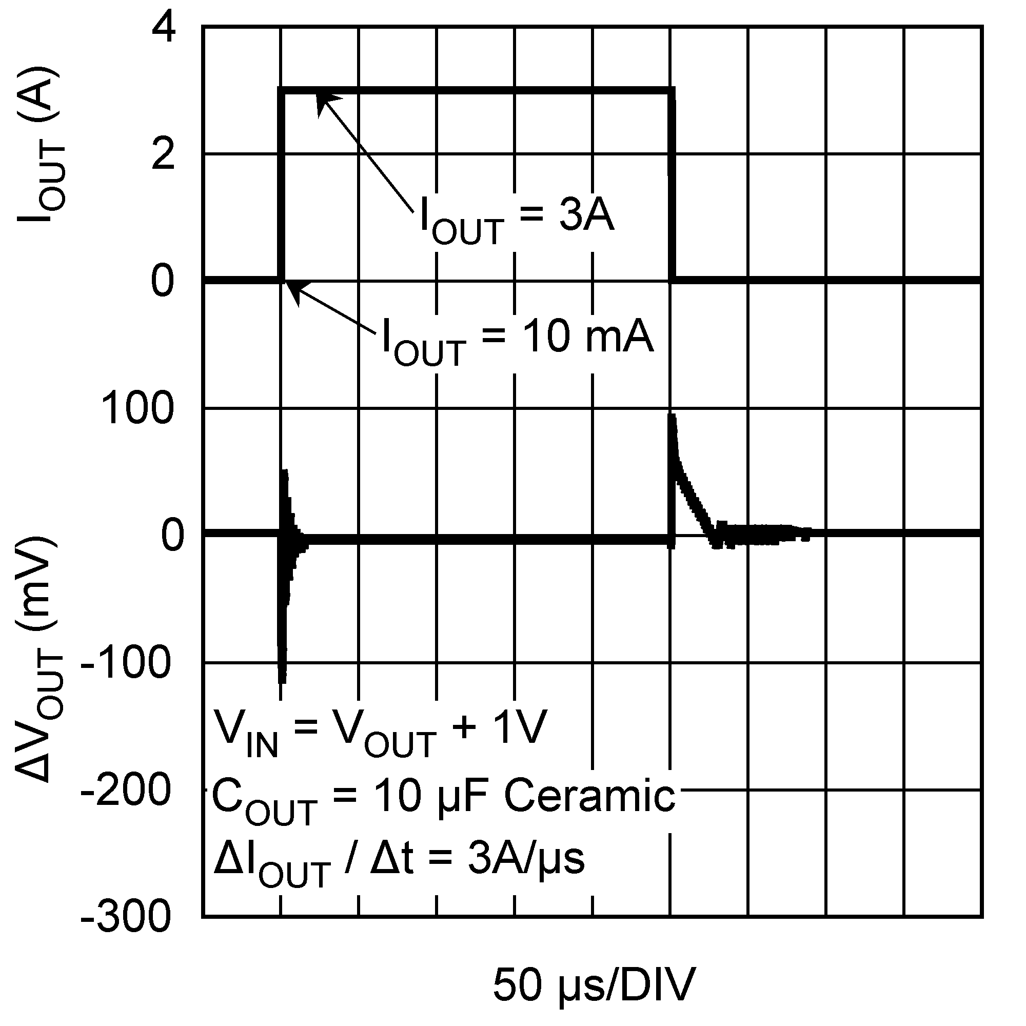
| COUT = 10-µF ceramic | ||
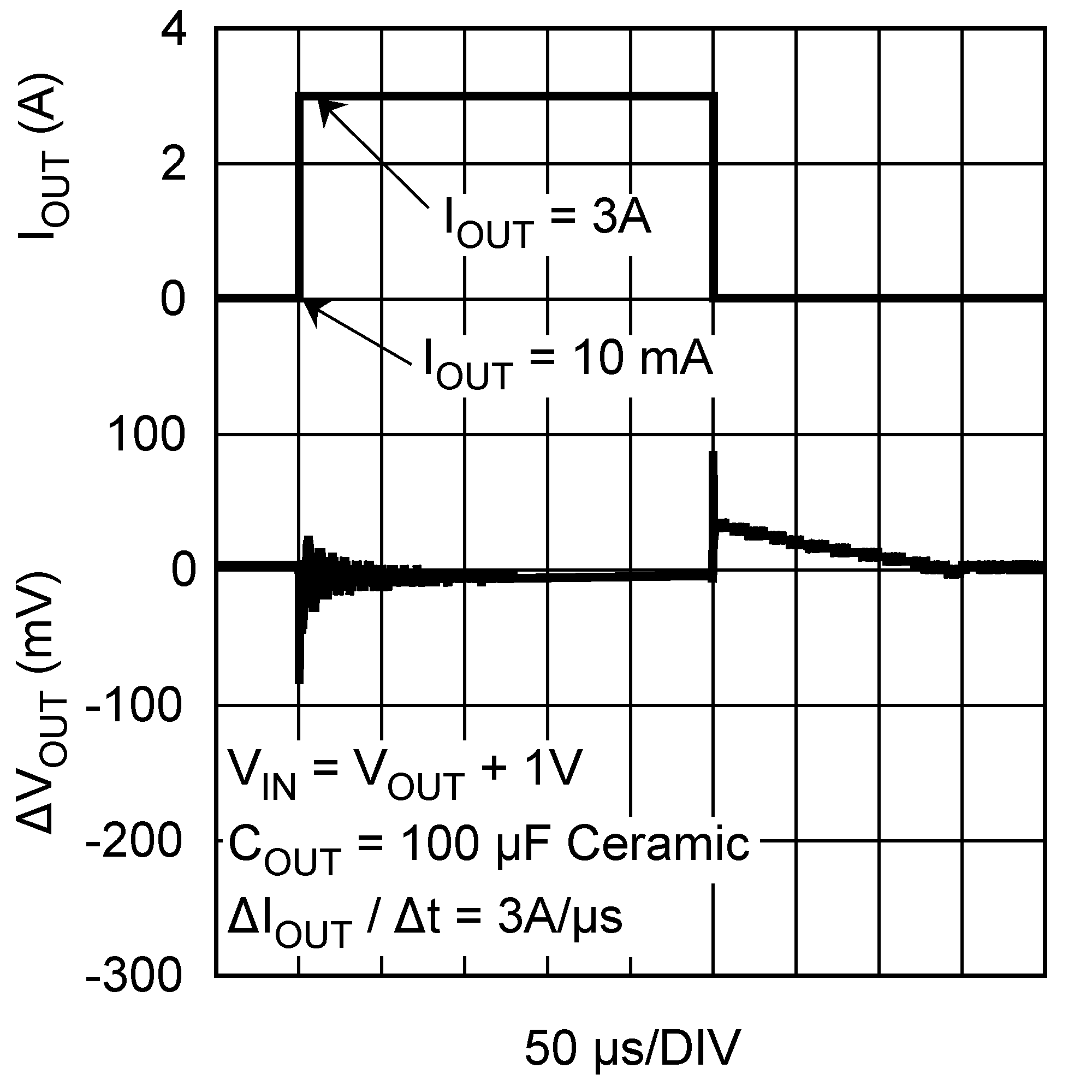
| COUT = 100-µF ceramic | ||
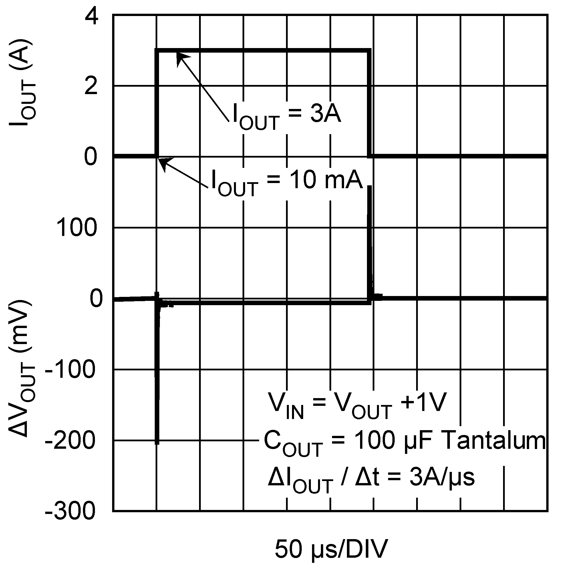
| COUT = 100-µF tantalum | ||
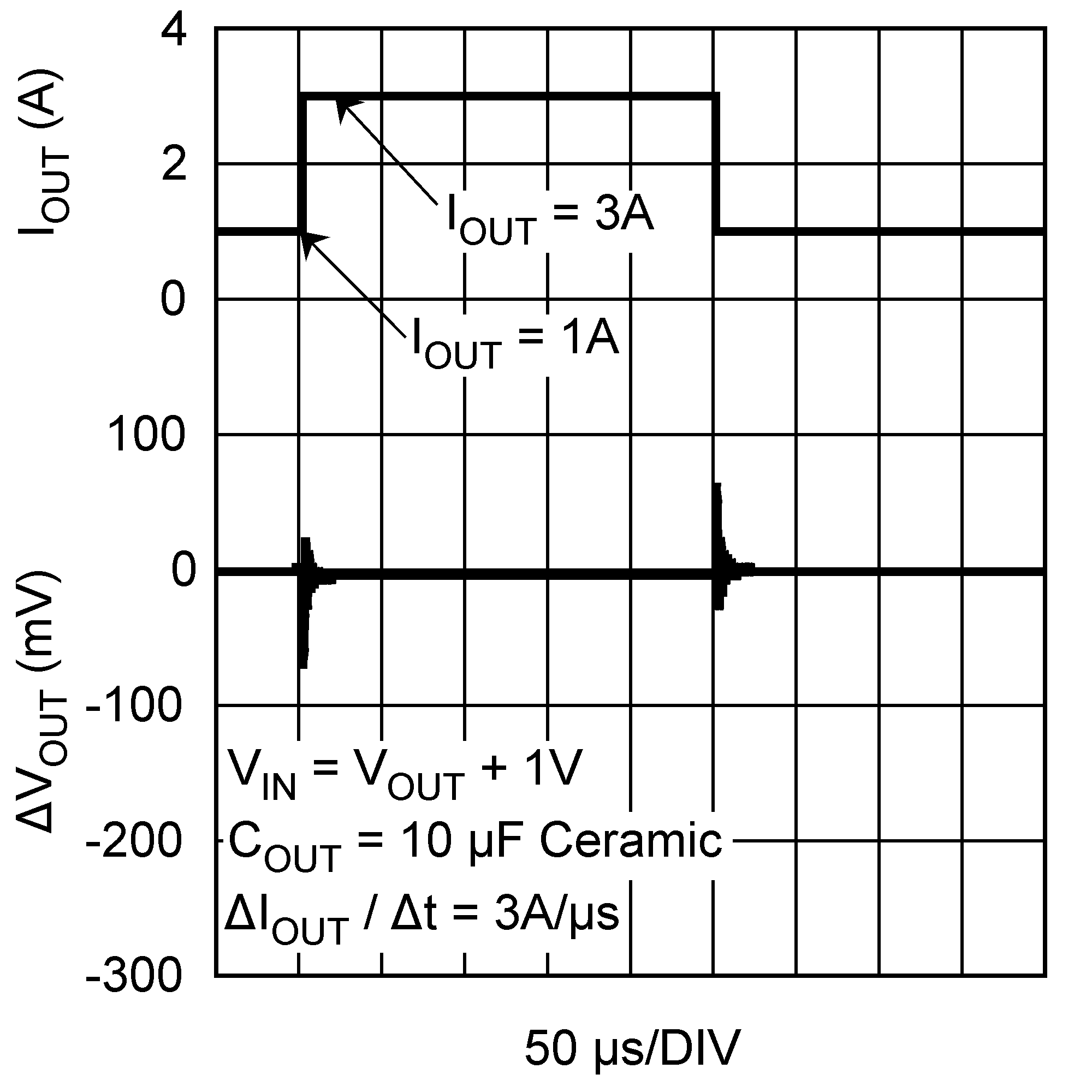
| COUT = 10-µF ceramic | ||
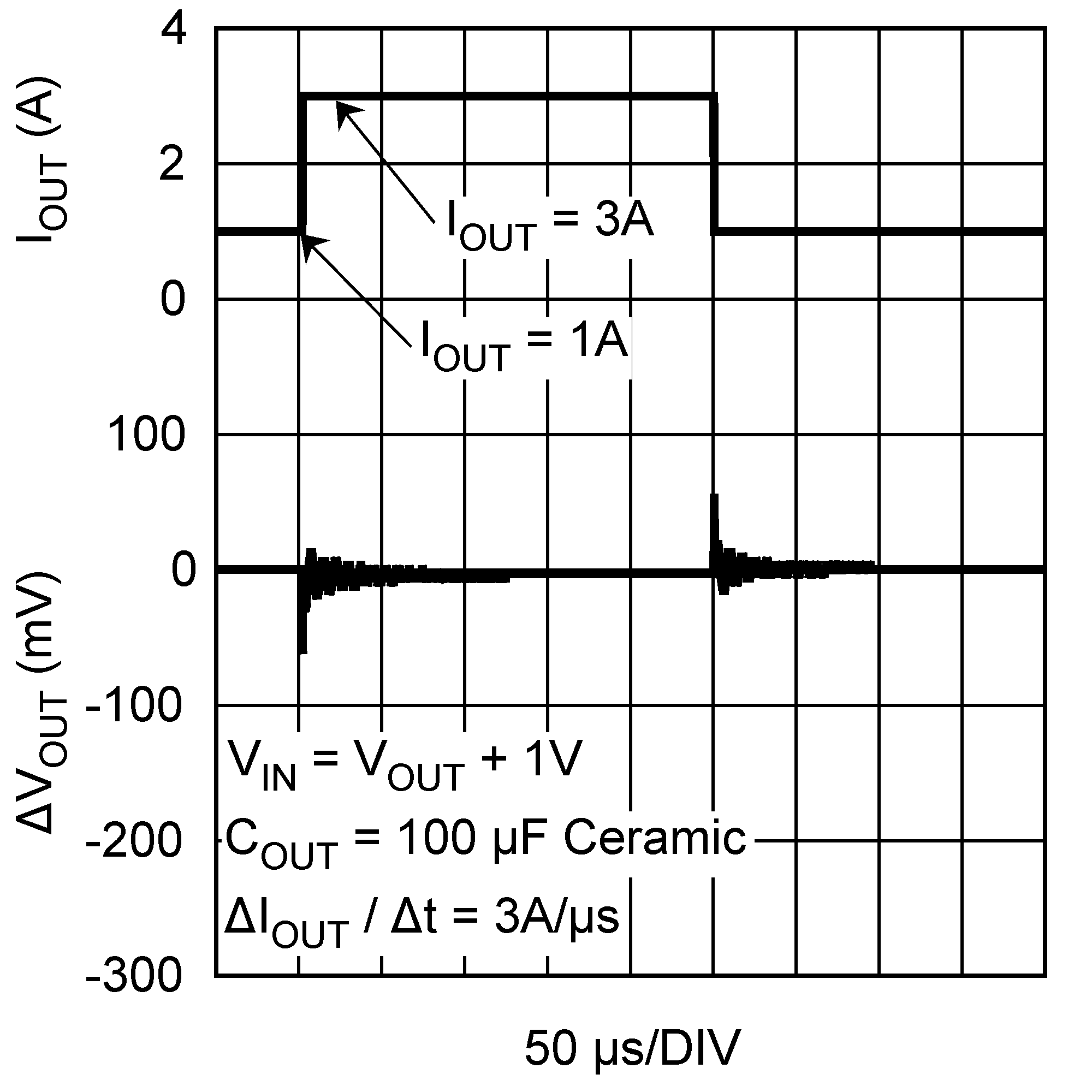
| COUT = 100-µF ceramic | ||
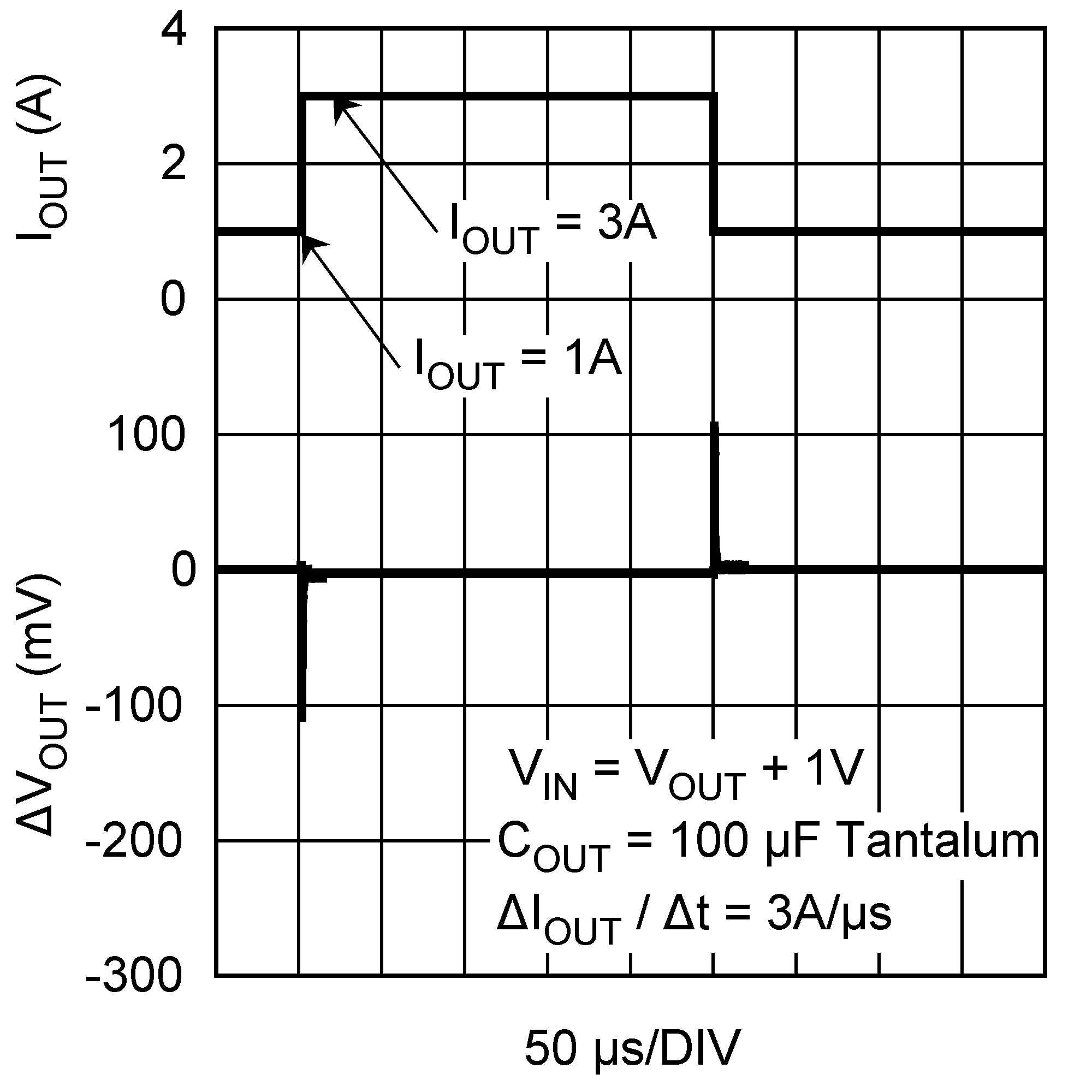
| COUT = 100-µF tantalum | ||