Unless otherwise specified: TA =
25°C, VIN = VO(NOM) + 1 V, COUT = 10 µF, CIN = 1
µF all voltage options, ON/ OFF pin tied to VIN.

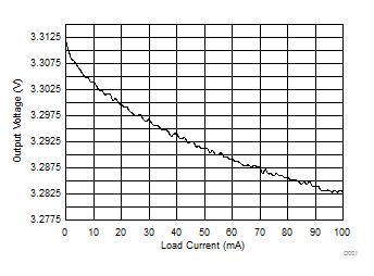
| VIN = 4.3 V, VOUT = 3.3 V |
Figure 5-1 Output Voltage
vs Load Current (Legacy Chip)
| VIN = 4.3 V, VOUT = 3.3 V |
Figure 5-3 Load Regulation
vs Temperature (New Chip) Figure 5-5 Output Voltage
vs VIN (New Chip)
 Figure 5-7 Line Regulation
vs VIN and Temperature (New Chip)
 Figure 5-9 Dropout Voltage
(VDO) vs Load Current (New Chip)
 Figure 5-11 Ground Pin
Current (IGND) vs Load Current (New Chip)
| VOUT = 3.3 V, IL = 100 mA |
Figure 5-13 Line Transient
Response (New Chip)
| VOUT = 3.3 V, COUT = 2.2 μF |
Figure 5-15 Load Transient
Response (New Chip) Figure 5-17 Short Circuit
Current vs Time (New Chip)
 Figure 5-19 Short Circuit
Current vs Output Voltage (VOUT) (New Chip)
 Figure 5-21 Ripple
Rejection vs Output Capacitor (CL) and Frequency (New Chip)
 Figure 5-23 Output Noise
Density vs Output Capacitor (CL) Frequency (New Chip)
| VOUT = 3.3 V, RL = 3.3 kΩ |
Figure 5-25 Turn-on
Waveform (New Chip) Figure 5-27 ON/
OFF Pin Current vs VON/ OFF (New
Chip)
 Figure 5-29 ON/
OFF Threshold vs Temperature (New Chip)
| VIN = 4.3 V, VOUT = 3.3 V |
Figure 5-2 Output Voltage
vs Load Current (New Chip)
| VIN = 4.3 V, VOUT = 3.3 V |
Figure 5-4 Output Voltage
vs Temperature (New Chip) Figure 5-6 Output Voltage
vs VIN and Temperature (New Chip)
 Figure 5-8 Dropout Voltage
(VDO) vs Temperature (New Chip)
 Figure 5-10 Ground Pin
Current (IGND) vs Temperature (New Chip)
| VOUT = 3.3 V, RL = 3.3 kΩ |
Figure 5-12 Input Current
vs Input Voltage (VIN) (New Chip) Figure 5-14 Line Transient
Response (New Chip)
 Figure 5-16 Short Circuit
Current vs Time (New Chip)
 Figure 5-18 Instantaneous
Short Circuit Current vs Temperature (New Chip)
 Figure 5-20 Ripple
Rejection vs Load Current (IL) and Frequency (New Chip)
 Figure 5-22 Output Noise
Density vs Load Current (IL) Frequency (New Chip)
 Figure 5-24 Output Reverse
Leakage vs Temperature (New Chip)
 Figure 5-26 Turn-off
Waveform (New Chip)
 Figure 5-28 ON/
OFF Pin Current vs VON/ OFF (New
Chip)


