ZHCSIE8C June   2018  – October 2020 LMR33630-Q1

PRODUCTION DATA  

  1. 特性
  2. 应用
  3. 说明
  4. Revision History
  5. Pin Configuration and Functions
  6. Specifications
    1. 6.1 Absolute Maximum Ratings
    2. 6.2 ESD Ratings
    3. 6.3 Recommended Operating Conditions
    4. 6.4 Thermal Information
    5. 6.5 Electrical Characteristics
    6. 6.6 Timing Characteristics
    7. 6.7 System Characteristics
    8. 6.8 Typical Characteristics
  7. Detailed Description
    1. 7.1 Overview
    2. 7.2 Functional Block Diagram
    3. 7.3 Feature Description
      1. 7.3.1 Power-Good Flag Output
      2. 7.3.2 Enable and Start-up
      3. 7.3.3 Current Limit and Short Circuit
      4. 7.3.4 Undervoltage Lockout and Thermal Shutdown
    4. 7.4 Device Functional Modes
      1. 7.4.1 Auto Mode
      2. 7.4.2 Dropout
      3. 7.4.3 Minimum Switch On-Time
  8. Application and Implementation
    1. 8.1 Application Information
    2. 8.2 Typical Application
      1. 8.2.1 Design Requirements
      2. 8.2.2 Detailed Design Procedure
        1. 8.2.2.1  Custom Design With WEBENCH® Tools
        2. 8.2.2.2  Choosing the Switching Frequency
        3. 8.2.2.3  Setting the Output Voltage
        4. 8.2.2.4  Inductor Selection
        5. 8.2.2.5  Output Capacitor Selection
        6. 8.2.2.6  Input Capacitor Selection
        7. 8.2.2.7  CBOOT
        8. 8.2.2.8  VCC
        9. 8.2.2.9  CFF Selection
        10. 8.2.2.10 External UVLO
        11. 8.2.2.11 Maximum Ambient Temperature
      3. 8.2.3 Application Curves
    3. 8.3 What to Do and What Not to Do
  9. Power Supply Recommendations
  10. 10Layout
    1. 10.1 Layout Guidelines
      1. 10.1.1 Ground and Thermal Considerations
    2. 10.2 Layout Example
  11. 11Device and Documentation Support
    1. 11.1 Device Support
      1. 11.1.1 Development Support
        1. 11.1.1.1 Custom Design With WEBENCH® Tools
    2. 11.2 Documentation Support
      1. 11.2.1 Related Documentation
    3. 11.3 支持资源
    4. 11.4 接收文档更新通知
    5. 11.5 Trademarks
    6. 11.6 静电放电警告
    7. 11.7 术语表

封装选项

请参考 PDF 数据表获取器件具体的封装图。

机械数据 (封装 | 引脚)
  • RNX|12
散热焊盘机械数据 (封装 | 引脚)
订购信息

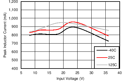
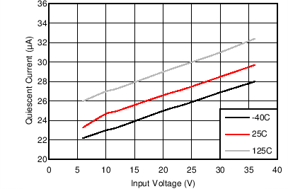
Typical Characteristics

Unless otherwise specified the following conditions apply: TA = 25°C and VIN = 12 V
GUID-723915C8-A91B-4DDC-965A-DF94BE2B06A9-low.png
VFB = 1.2 V
Figure 6-1 Non-Switching Input Supply Current
GUID-E845428A-AA34-46BE-BA65-F77CC711CA77-low.png
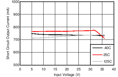
VOUT = 0 V ƒS = 400 kHz See Figure 8-29
Figure 6-3 Short-Circuit Output Current
GUID-B7889875-2662-4129-AEBA-D1F70C5050DC-low.gif
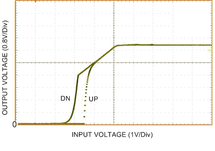
IOUT = 1 mA See Figure 8-29
Figure 6-5 UVLO Thresholds
GUID-929DB695-774F-41F7-8E09-FFAF1DE04C98-low.png
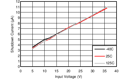
EN = 0 V
Figure 6-2 Shutdown Supply Current
GUID-5161C390-D41D-457B-A9A5-538B6D5310F5-low.png
 
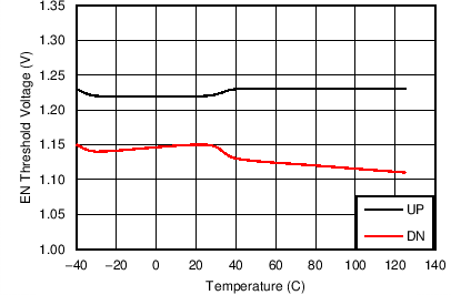
Figure 6-4 Precision Enable Thresholds
GUID-0533885D-0B47-4919-8199-4EFBEB35C98A-low.png
IOUT = 0 A VOUT = 5 V See Figure 8-29
ƒSW = 400 kHz
Figure 6-6 IPEAK-MIN