ZHCSFR2B December   2016  – March 2018 LMR23630-Q1

PRODUCTION DATA.  

  1. 特性
  2. 应用
  3. 说明
    1.     Device Images
      1.      简化原理图
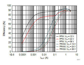
      2.      效率与负载间的关系,VIN = 12V,PFM 选项
  4. 修订历史记录
  5. Product Portfolio
  6. Pin Configuration and Functions
    1.     Pin Functions
  7. Specifications
    1. 7.1 Absolute Maximum Ratings
    2. 7.2 ESD Ratings
    3. 7.3 Recommended Operating Conditions
    4. 7.4 Thermal Information
    5. 7.5 Electrical Characteristics
    6. 7.6 Timing Characteristics
    7. 7.7 Switching Characteristics
    8. 7.8 Typical Characteristics
  8. Detailed Description
    1. 8.1 Overview
    2. 8.2 Functional Block Diagram
    3. 8.3 Feature Description
      1. 8.3.1  Fixed-Frequency Peak-Current-Mode Control
      2. 8.3.2  Adjustable Frequency
      3. 8.3.3  Adjustable Output Voltage
      4. 8.3.4  Enable/Synchronization
      5. 8.3.5  VCC, UVLO
      6. 8.3.6  Minimum ON-time, Minimum OFF-time and Frequency Foldback at Dropout Conditions
      7. 8.3.7  Power Good (PGOOD)
      8. 8.3.8  Internal Compensation and CFF
      9. 8.3.9  Bootstrap Voltage (BOOT)
      10. 8.3.10 Overcurrent and Short-Circuit Protection
      11. 8.3.11 Thermal Shutdown
    4. 8.4 Device Functional Modes
      1. 8.4.1 Shutdown Mode
      2. 8.4.2 Active Mode
      3. 8.4.3 CCM Mode
      4. 8.4.4 Light Load Operation (PFM Option)
      5. 8.4.5 Light Load Operation (FPWM Option)
  9. Application and Implementation
    1. 9.1 Application Information
    2. 9.2 Typical Applications
      1. 9.2.1 Design Requirements
      2. 9.2.2 Detailed Design Procedure
        1. 9.2.2.1  Custom Design With WEBENCH® Tools
        2. 9.2.2.2  Output Voltage Setpoint
        3. 9.2.2.3  Switching Frequency
        4. 9.2.2.4  Inductor Selection
        5. 9.2.2.5  Output Capacitor Selection
        6. 9.2.2.6  Feed-Forward Capacitor
        7. 9.2.2.7  Input Capacitor Selection
        8. 9.2.2.8  Bootstrap Capacitor Selection
        9. 9.2.2.9  VCC Capacitor Selection
        10. 9.2.2.10 UVLO Setpoint
      3. 9.2.3 Application Curves
  10. 10Power Supply Recommendations
  11. 11Layout
    1. 11.1 Layout Guidelines
      1. 11.1.1 Compact Layout for EMI Reduction
      2. 11.1.2 Ground Plane and Thermal Considerations
      3. 11.1.3 Feedback Resistors
    2. 11.2 Layout Examples
  12. 12器件和文档支持
    1. 12.1 使用 WEBENCH® 工具创建定制设计
    2. 12.2 接收文档更新通知
    3. 12.3 社区资源
    4. 12.4 商标
    5. 12.5 静电放电警告
    6. 12.6 Glossary
  13. 13机械、封装和可订购信息

封装选项

机械数据 (封装 | 引脚)
散热焊盘机械数据 (封装 | 引脚)
订购信息

Typical Characteristics

Unless otherwise specified the following conditions apply: VIN = 12 V, fSW = 400 kHz, L = 8.2 µH, COUT = 150 µF, TA = 25°C.
LMR23630-Q1 D001_SNVSAH2.gif
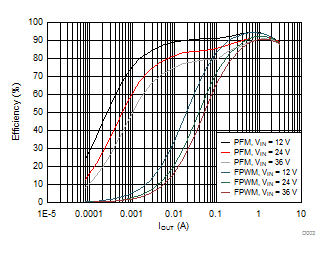
fSW = 400 kHz VOUT = 5 V
Figure 1. Efficiency vs Load Current
LMR23630-Q1 D003_SNVSAH2.gif
fSW = 200 kHz (Sync) VOUT = 5 V
Figure 3. Efficiency vs Load Current
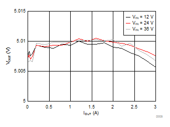
LMR23630-Q1 D005_SNVSAH2.gif
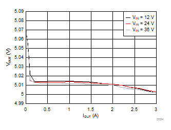
PFM Option VOUT = 5 V
Figure 5. Load Regulation
LMR23630-Q1 D007_SNVSAH2.gif
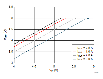
VOUT = 5 V
Figure 7. Dropout Curve
LMR23630-Q1 D009_SNVSAH2.gif
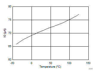
VIN = 12 V VFB = 1.1 V
Figure 9. IQ vs Junction Temperature
LMR23630-Q1 D011_SNVSAH2.gif
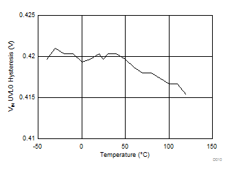
Figure 11. VIN UVLO Hysteresis vs Junction Temperature
LMR23630-Q1 D002_SNVSAH2.gif
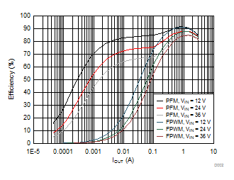
fSW = 400 kHz VOUT = 3.3 V
Figure 2. Efficiency vs Load Current
LMR23630-Q1 D004_SNVSAH2.gif
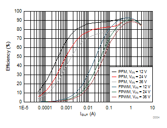
fSW = 200 kHz (Sync) VOUT = 3.3 V
Figure 4. Efficiency vs Load Current
LMR23630-Q1 D006_SNVSAH2.gif
FPWM Option VOUT = 5 V
Figure 6. Load Regulation
LMR23630-Q1 D008_SNVSAH2.gif
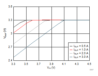
VOUT = 3.3 V
Figure 8. Dropout Curve
LMR23630-Q1 D010_SNVSAH2.gif
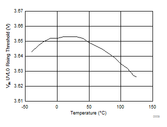
Figure 10. VIN UVLO Rising Threshold vs Junction Temperature
LMR23630-Q1 D012_SNVSAH2.gif
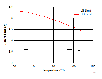
VIN = 12 V
Figure 12. HS and LS Current Limit vs Junction Temperature