ZHCSC60A March 2014 – September 2014 LMP93601
PRODUCTION DATA.
- 1 特性
- 2 应用范围
- 3 说明
- 4 简化热电堆阵列系统图
- 5 修订历史记录
- 6 Pin Configuration and Functions
- 7 Specifications
-
8 Detailed Description
- 8.1 Overview
- 8.2 Functional Block Diagram
- 8.3
Feature Description
- 8.3.1 Data Format
- 8.3.2 Transfer Function
- 8.3.3 Input Routing Mux
- 8.3.4 Programmable Gain Amplifier
- 8.3.5 PGA Bypass Mode
- 8.3.6 Over-Range Detection
- 8.3.7 Analog-To-Digital Converter (ADC)
- 8.3.8 Programmable Digital Filters
- 8.3.9 Common Mode Voltage Generator
- 8.3.10 Low Drop-Out Regulator (LDO)
- 8.3.11 External Clock
- 8.3.12 Operating Modes
- 8.3.13 Data Ready Function (DRDYB)
- 8.3.14 Synchronous Serial Peripheral Interface (SPI)
- 8.3.15 Power Management Mode; Standby, Conversion and Shutdown
- 8.3.16 Power-On Sequence and Reset (POR) Function
- 8.3.17 Brown-Out Detection Function
- 8.3.18 Reset Function
- 8.4 Device Functional Modes
- 8.5 Programming
- 8.6 Register Maps
- 8.7 Multi Byte Access (Auto Increment) Mode
- 8.8 Multi-Channel Data Read
- 9 Application and Implementation
- 10Power Supply Recommendations
- 11Layout
- 12器件和文档支持
- 13机械封装和可订购信息
9 Application and Implementation
NOTE
Information in the following applications sections is not part of the TI component specification, and TI does not warrant its accuracy or completeness. TI’s customers are responsible for determining suitability of components for their purposes. Customers should validate and test their design implementation to confirm system functionality.
9.1 Application Information
Micro-electro-mechanical systems (MEMS) thermopile sensor arrays are gaining popularity in building automation applications for efficient control of heating, ventilation, and air conditioning (HVAC) system in residential and commercial buildings. The sensors are installed in the building rooms for detecting the presence and the motion of the occupants in the rooms. Depending on the presence or absence of people in the room, the HVAC system is turned on or off respectively. In addition, the thermopile sensor are used for detecting flow of air in the in the duct-work system in the buildings.
A typical MEMS thermopile array sensor consists of a number of thermopile elements arranged in a matrix configuration. Each element of the array is accessed by selecting the corresponding XY address in the array using internal or external decoder circuits. An output frame consists of differential signals form X by Y elements. Each frame is transferred to the analog-front-end via OUTP (positive output) and OUTN (negative output) output pins of the sensor in serial format. The analog output signal of the MEMS thermopile sensor is in the micro volt range. It needs to be amplified significantly before made available to the input of an ADC for digitization.
9.2 Typical Applications
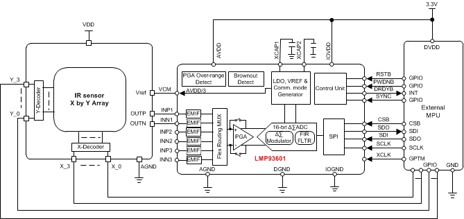 Figure 29. LMP93601 Thermopile Array Interface
9.2.1 Design Requirements
The application requires a microcontroller (MCU) such as Texas Instruments MSP430x, or TM4C129x series of MCUs connected via Synchronous Serial Interface (SPI) to the LMP93601 AFE. As shown in Figure 29, the X and Y decoder lines of the thermopile sensor (transducer) needs to be interfaced to the GPIO (General Purpose Input Output) pins of the MCU. The LMP93601 would require an external clock signal of 4 MHz (±3%).The timer subsystem of the MCU is well suited to generate the clock signal. A timer output pin shall be used to interface the output of the MCU timer to the XCLK pin of the LMP93601.
The device provides a reference voltage output (VCM) source to center the output of the sensor around AVDD/3. If the sensor does not provide a reference input pin, the INPx, INNx inputs of the LMP93601 should be connected (pulled-up) to VCM output via 2.2 MΩ resistors.
The data converter of the LMP93601 is an incremental delta-sigma type ADC, the modulator is reset after every conversion. Therefore, after each thermopile element is sampled and the ADC modulator goes through a reset, there is no possibility of any trace of signal from the previously sampled element.
To sample each thermopile element in the sensor array, the X and Y decoder signals must be provided over the GPIO, then firmware should allow settling of the data on the decoder. The SYNC pin is provided to signal the beginning of conversion to LMP93601 ADC. A GPIO of the MCU needs to be interfaced to the SYNC input pin of the LMP93601 for this purpose.
9.2.2 Detailed Design Procedure
In thermopile array systems, settling time of the signal path plays an important role when higher frame transfer rates are desired. A frame is an array of X by Y thermopile elements. While the data from each pixel is being transferred out of the sensor in a sequence, the MUX output must settle to the proper voltage from the element in the array that is being accessed. The total analog signal path settling time is determined by combined sensor’s settling time (tssnsr) and AFE’s settling time (tsafe). The settling time is determined by the sum of capacitances of the following: pixel in the array, sensor’s MUX, AFE’s MUX, PCB, AFE’s input stage, and sensor’s resistance.
To achieve faster settling time, total capacitance in the signal path should be kept as low as possible. Therefore, the system designers should take the resistance of the sensor and the related capacitance into consideration to achieve optimal performance of the signal path. For example, the pixel-to-pixel settling time should be keep below 70 μs to process five frame per second (1326 SPS) using a 16 x 16 array sensor. A simplified thermopile array sensor equivalent circuit is shown in Figure 30.
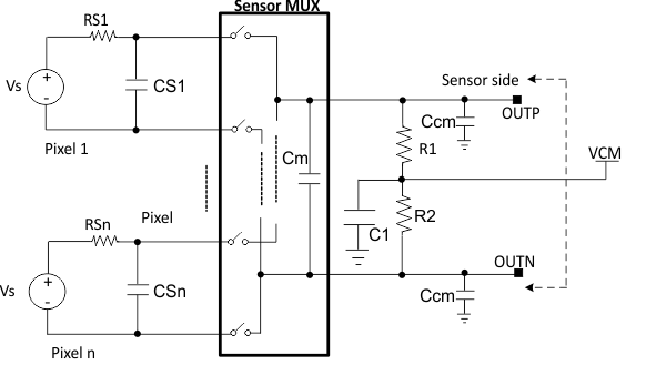 Figure 30. Simplified Thermopile Sensor Array
The value of biasing resistors; R1 and R2, should be much higher than the value of the sensor output resistance RSx (that is, R1 = R2 > 10 * RSx).
The bias current of the sensor and the leakage current of the sensor’s MUX should be considered as well. In Figure 31 R1 and R2 need to be matched closely to avoid introduction of differential offset error voltage in the signal path due to mismatched current flow through these resistors. Moreover, Ios through RSx needs to be calibrated out over temperature. To simplify the circuit in Figure 31 the MUX inside the AFE is not shown.
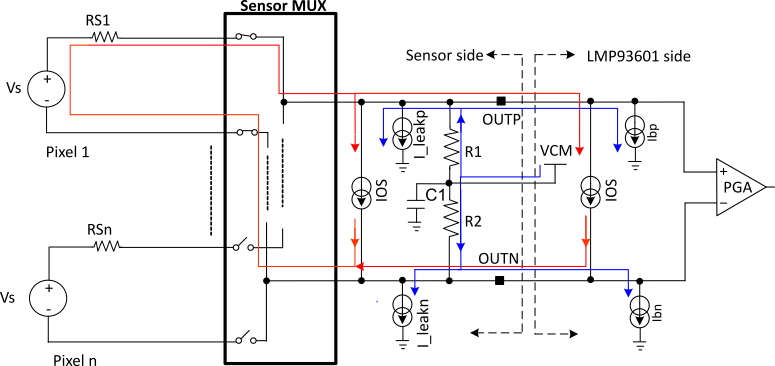 Figure 31.