ZHCSC60A March 2014 – September 2014 LMP93601
PRODUCTION DATA.
- 1 特性
- 2 应用范围
- 3 说明
- 4 简化热电堆阵列系统图
- 5 修订历史记录
- 6 Pin Configuration and Functions
- 7 Specifications
-
8 Detailed Description
- 8.1 Overview
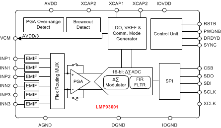
- 8.2 Functional Block Diagram
- 8.3
Feature Description
- 8.3.1 Data Format
- 8.3.2 Transfer Function
- 8.3.3 Input Routing Mux
- 8.3.4 Programmable Gain Amplifier
- 8.3.5 PGA Bypass Mode
- 8.3.6 Over-Range Detection
- 8.3.7 Analog-To-Digital Converter (ADC)
- 8.3.8 Programmable Digital Filters
- 8.3.9 Common Mode Voltage Generator
- 8.3.10 Low Drop-Out Regulator (LDO)
- 8.3.11 External Clock
- 8.3.12 Operating Modes
- 8.3.13 Data Ready Function (DRDYB)
- 8.3.14 Synchronous Serial Peripheral Interface (SPI)
- 8.3.15 Power Management Mode; Standby, Conversion and Shutdown
- 8.3.16 Power-On Sequence and Reset (POR) Function
- 8.3.17 Brown-Out Detection Function
- 8.3.18 Reset Function
- 8.4 Device Functional Modes
- 8.5 Programming
- 8.6 Register Maps
- 8.7 Multi Byte Access (Auto Increment) Mode
- 8.8 Multi-Channel Data Read
- 9 Application and Implementation
- 10Power Supply Recommendations
- 11Layout
- 12器件和文档支持
- 13机械封装和可订购信息
8 Detailed Description
8.1 Overview
The LMP93601 Analog-Front-End is a unique device designed from ground up specifically for interfacing to 16 x 16 MEMS (Micro-electro-mechanical systems) thermopile arrays, and thermopile mass flow sensors with very low output signals in the range of 1 µV to 600 µV. For signal conditioning of thermopile sensors, the AFE is required to have very low noise performance, very low offset voltage, very high gain, and low-power consumption at sampling rates to process several frames per second.
The signal chain includes a PGA featuring low offset voltage (0.7 µVrms), low input bias current (–1.3 nA), and programmable gain of 1x, 16x, 32x, 64x and 128x. The total gain of the signal path combined with the programmable digital gain of the 16-bit Delta-Sigma data converter is up to 4096x.
The signal chain features excellent total noise performance of below 0.5 uVrms at programmable sampling rates of up to 1.3 kSPS, while providing optimal power consumption during full operation (1.1 mA). The device features ultra-low shutdown current (0.1 µA), and standby mode current of 250 µA.
Other features include Low EMI sensitivity due to EMI hardened input stage, Internal reference voltage for the ADC, output reference voltage for thermopile sensors (VCM), a brown-out detector for low-battery condition, synchronous serial communication (SPI) communication up to 20 MHz, flex routing multiplexer for interfacing to multiple flow sensors, and PGA over range detection.
8.2 Functional Block Diagram
8.3 Feature Description
8.3.1 Data Format
The LMP93601 provides 16 bits of data in binary two's complement format. The positive full-scale input produces an output code of 7FFFh and the negative full-scale input produces an output code of 8000h. The output clips at these codes for signals that exceed full-scale (FS). Table 2 summarizes the ideal output codes for different input signals.
8.3.2 Transfer Function
The ADC output code in decimal is given by the relation:
Table 2. Example of ADC Output Code
| CODE (HEX) | CODE (DEC) | PGA (V/V) | DG (V/V) | VDIF (V) |
|---|---|---|---|---|
| 1946 | 6470 | 64 | 1 | 7.404E-3 |
| 3000 | 12288 | 16 | 4 | 14.063E-3 |
| D0FC | -12036 | 16 | 1 | -55.096E-3 |
| FFFC | -4 | 64 | 1 | -4.578E-6 |
8.3.3 Input Routing Mux
The LMP93601 offers 5 differential input channel configurations for its 3 differential input pairs:
- For 1-ch system: One of the 3 channels, Ch1, Ch2, or Ch3 is enabled
- For 2-ch system: Ch1 & Ch2 are enabled
- For 3-ch system: Ch1, Ch2, Ch3 are enabled
8.3.4 Programmable Gain Amplifier
The PGA provides a high input impedance to interface with signal sources that may have relatively high output impedance, such as thermopiles. The Programmable Gain amplifier gain can be programmed to 16, 32 64, and 128 V/V.
The maximum differential input voltage (Vdiff) of the PGA is ±64 mV when the programmed analog gain is 16 V/V. With analog gain programmed to 64V/V the maximum differential input voltage of the PGA is ±16 mV.
The input common mode voltage range of the PGA is AGND+0.3+Vdiff*Gain/2 to AVDD-1.40-Vdiff*Gain/2.
The PGA also has an EMIRR filter incorporated. The EMIRR filter is a single pole roll off providing enhanced noise immunity for unwanted RF signals.
8.3.5 PGA Bypass Mode
The PGA can be bypassed to access the 16 bit Delta-Sigma modulator directly. This mode results in a typical gain of 1 V/V at a supply current of typically 230 µA. The input common mode range in the PGA-bypass mode is rail to rail and the maximum differential input voltage that can be applied to the Delta-Sigma modulator is ± 1.2 Vpp differential. The typical noise at 1057 SPS is 20 uVrms. Typical input impedance in the PGA bypass mode is 1.3 MΩ//7 pF. In the PGA-bypass mode, the PGA and overrange detectors are disabled. To access the PGA-bypass mode the following SPI write sequence must be followed in this exact order:
Table 3. PGA Bypass Mode SPI Write Sequence
| ADDRESS | WRITE | DESCRIPTION | ||
|---|---|---|---|---|
| 0x1 | Program as normal | |||
| 0x02 | Program as normal | |||
| 0x03 | See Table 4 below | |||
| 0x05 | 8'h01 | Mask PGA OR detectors (else the conversion will read 7FFF) | ||
| 0x60 | 8'h93 | First write to address 0x60 | ||
| 0x60 | 8'h60 | Second write to address 0x60 | ||
| 0x63 | 8'h10 | Override | ||
| 0x61 | 8'h28 | PGA bypass and OR detectors shutdown | ||
| 0x04 | 8'h01 | Conversion mode | ||
| 0x00 | 8'h01 | lock | ||
Table 4. PGA Bypass Register 0x03 Setting Description
| ADDR [6:0] | NAME | # OF BITS | TYPE | DEFAULT | DESCRIPTION |
|---|---|---|---|---|---|
| 0x03 | Config3 | 5 | R/W | 8’h52 | PGA settings for differential channels [6:4] Digital 3’b000: 1 3’b001: 2 3’b010: 4 3’b011: 8 3’b100: 16 3’b101: 32(default) 3’b110-111: Reserved [1:0] Analog 2’b00: 16 2’b01: 32 2’b10: 64 (default) 2’b11: 128 [7] always 0 [2] Bypass PGA, bit [1:0] would be ignored |
To exit the PGA-bypass mode, a reset is required, either via the RSTB or SPI. Failure to follow this exact sequence may result in the device becoming unresponsive, thereby requiring a reset, either via the RSTB or SPI.
8.3.6 Over-Range Detection
The PGA has over-range detection and when signals are outside the minimum or maximum allowed signal, an out of range condition will be reported as “0x7FFF” for the corresponding channel. A status register provides further details of the out of range condition. The overrange detectors are at the output of the PGA and check for five conditions:
- PGA positive output low
- PGA negative output low
- PGA positive output high
- PGA negative output high
- PGA differential output high
The “output high” overrange detectors typically trip at AVDD-1.28 V. Both “output low” overrange detectors typically trip at 0.11 V and the differential overrange detector is typically at +1.22 and -1.22 V differential.
For example, if the input common mode is below 0.11 V and a zero differential voltage (shorted input) is applied, both the PGA positive and PGA negative “output low” detectors would trip. Likewise, if the input common mode is over AVDD-1.28 and a zero differential voltage (shorted input) is applied, both the PGA positive and PGA negative “output high” detectors would trip.
For the differential output high detector to trip, the output of the PGA has to be greater than 1.22 V or less than –1.22 V. At a gain of 64, this would translate to an input referred differential voltage of Vdiff = 1.22/64 = 19 mV
8.3.7 Analog-To-Digital Converter (ADC)
The 16 bit Sigma Delta Modulator (SDM) takes the output signal of the PGA and converts this signal into a high resolution bit stream that is further processed by the digital filters. The 2.4 V reference for the SDM is internally generated and requires a high-performance, low ESR (<0.1 Ω), and Low ESL(<1nH) 1uF (±10%) external bypass capacitor for optimal performance on the XCAP1 pin. This reference should not be used to drive external circuitry.
The SDM clock uses a divided-down external clock (XCLK).
8.3.8 Programmable Digital Filters
A programmable digital filter behind the SDM reconstructs the signal from the SDM output bit stream. The filter consists of programmable filter stages. Each of the stages further filters and decimates the bit stream so that the data rate and bandwidth of the signal is reduced and at the same time the resolution is enhanced.
An example of the filter response when programmed for 265, 530, 1057 or 1326 SPS is shown in Figure 16.
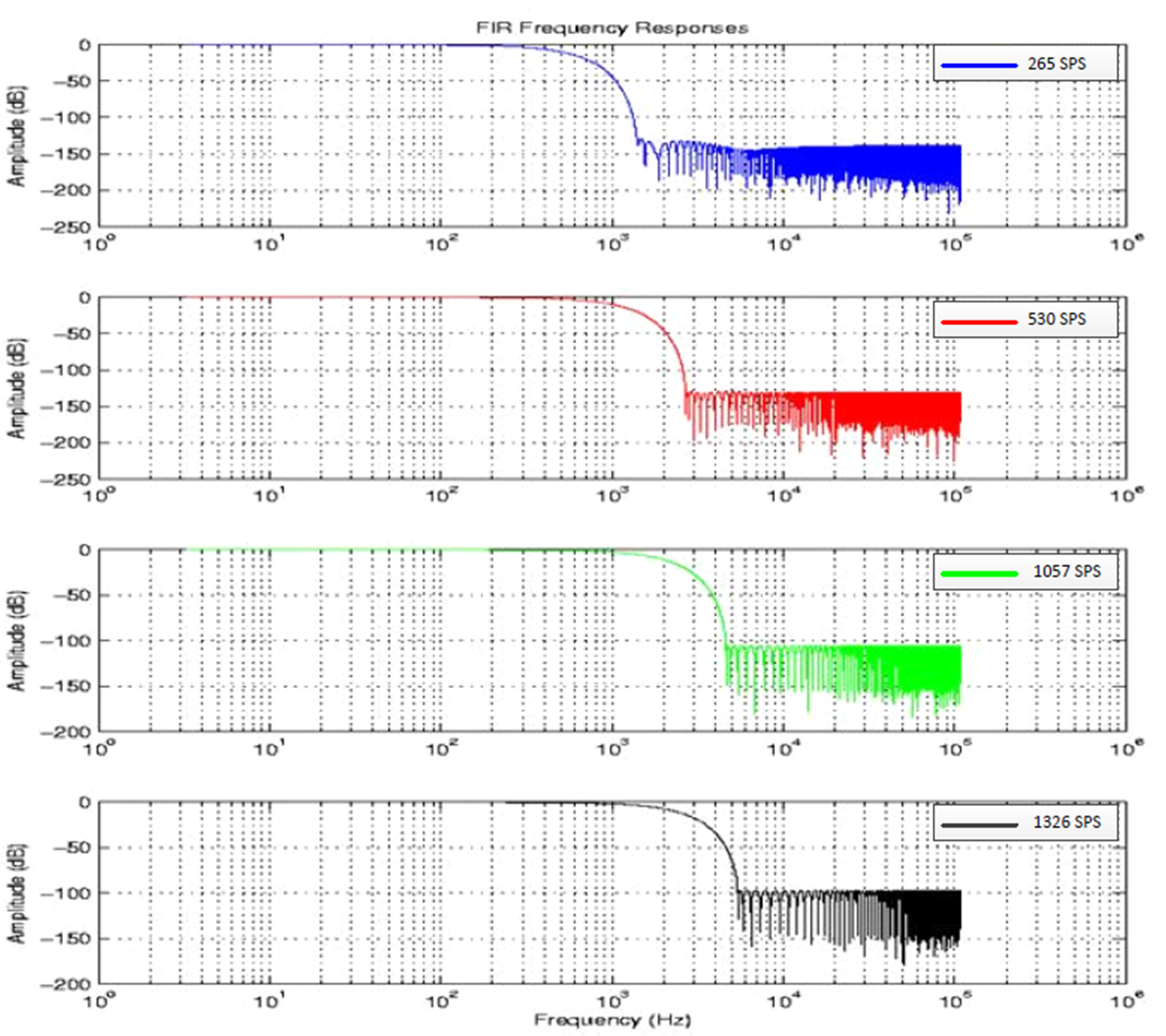 Figure 16. Bandwidth and Module Noise Performance
8.3.9 Common Mode Voltage Generator
The common mode reference generator (VCM) provides an AVDD/3 reference. It can drive a 100nF (±10%) external capacitance with typical ESR/ESL of 0.1 Ω and 1 nH. It can also be used to drive guard traces placed around the input PCB traces to reduce PCB leakage currents to the inputs. The VCM can be disabled with the Reference Enable register. In case the VCM is disabled, an external common mode voltage that tracks the common mode of the input channel(s) needs to be connected to the VCM pin to function as a reference for the over-range detection circuitry. In case the VCM is disabled, it is recommended to add an external 10 kΩ series resistor.
8.3.10 Low Drop-Out Regulator (LDO)
The on chip LDO generates 1.2V for the digital core. A 100nF (+/-10%) external capacitance with low ESR/ESL (typical 0.1 ohm and 1 nH) is required on the XCAP2 pin to provide adequate supply bypass for the internal digital core. The LDO should not be used to drive external circuitry.
8.3.11 External Clock
The LMP93601 does not have an internal oscillator and needs an external clock, XCLK. The XCLK needs to be running all the time when the LMP93601 is operating. The SYNC, DRDYB, and RSTB are synchronous to XCLK. The LMP93601 operating range for XCLK is 3.6 to 4.4 MHz.
8.3.12 Operating Modes
The LMP93601 can be programmed to convert data in continuous-time or single shot modes.
8.3.13 Data Ready Function (DRDYB)
DRDYB is an active low output signal. It is asserted when new data is ready to be read and should be used by the MCU for data capturing.
When DRDYB is asserted, the MCU can capture the data any time before the next DRDYB is asserted. The time is defined as 1/ODR. Please note that if data is not read within the time period, it will be over-written internally in the LMP93601 by the new data.
For DRDYB de-assertion, it is normally cleared by a data read. In the following example: it is de-asserted on the 14th SCLK rising edge.
If data has not been read when the new data is about to be ready, DRDYB will be de-asserted for 15 XCLK periods (defined as tDRDYB) so that LMP93601 can re-assert the DRDYB. Once this happens, the µC should wait for the next DRDYB assertion before issuing an SPI read protocol.
DRDYB assertion and de-assertion is synchronous to XCLK and SCLK respectively in normal operation.
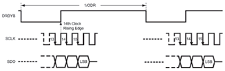 Figure 17. DRDYB Behavior for A Complete Read Operation
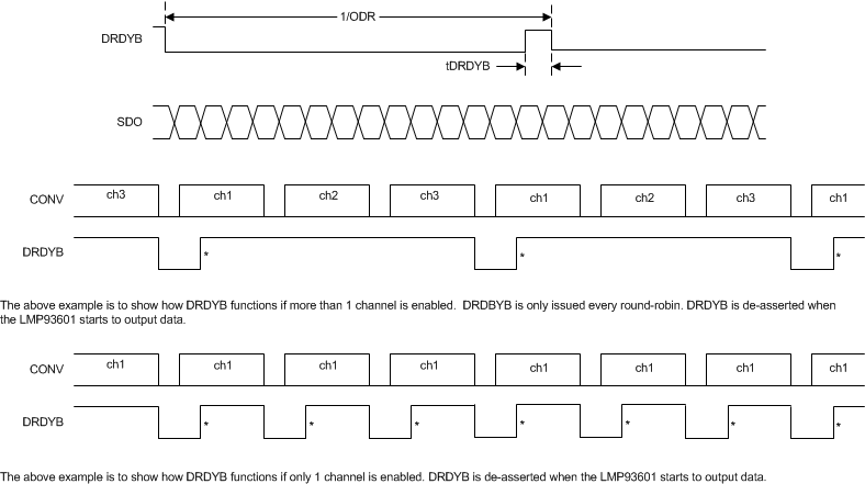 Figure 18. DRDYB Behavior for an Incomplete Read Operation
8.3.14 Synchronous Serial Peripheral Interface (SPI)
The serial peripheral interface (SPI) interface allows access to the control registers of the LMP93601. The serial interface is a generic 4-wire synchronous interface compatible with SPI type of interfaces used on many microcontrollers and DSP controllers. A typical serial interface access cycle is exactly 16 bits long, which includes an 8-bit command field (R/WB + 7-bit address) to provide a maximum of 128 direct access addresses, and an 8-bit data field.
LMP93601’s SCLK can be in either idle high or idle low state when CSB is de-asserted. The first incoming data on the SCLK rising edge, and all incoming data at SDI is captured on the SCLK rising edge. Outgoing data is sourced at SDO on the SCLK falling edge and the MCU can capture data from the LMP93601 on the SCLK rising edge.
8.3.15 Power Management Mode; Standby, Conversion and Shutdown
The device can be placed in Standby and Conversion mode via the SPI. In Conversion mode, the ADC and PGA are operating and converting data. In Standby mode the PGA and ADC are disabled and not converting data. In Standby mode the contents of the registers are unaffected, and there is a drastic power reduction. Only the internal reference, LDO, VCM driver and the digital are on.
The reaction time going from Standby mode to Conversion mode is approximately 100 µs.
The LMP93601 can be put in shutdown mode by taking the PWDNB pin low. In shutdown mode, all internal circuitry is disabled and no register settings are maintained. The power consumption is very low (< 0.1 uA). Releasing the PWDNB (taking it high) will “wake up” the device and it will return to the default Standby mode. Wake up time from shutdown can be up to 10 ms.
Table 5. Wake Up Time From Low Power Modes
| Mode | Registers | Power | Wake Up Time | Programmable via |
|---|---|---|---|---|
| Shutdown | Not maintained | ~0.1 µA | Less than 10 ms to go to Standby mode | PWDNB pin |
| Standby | Maintained | ~175 µA | ~100 µs to go to conversion mode | SPI |
| Conversion | Maintained | 1.1 mA | n/a | SPI |
8.3.16 Power-On Sequence and Reset (POR) Function
An internal power on reset is generated after both the internal LDO (to supply the internal digital) and IOVDD reach valid values. The internal LDO will reach stable values only after the AVDD has reached at least 2.7 V.
The device should be powered up with AVDD enabled and stabilized first, then the IOVDD. This allows the device to start in the default power up state and ensures that the internal power on reset is generated after both the internal LDO (to supply the internal digital) and IOVDD reach valid values. The internal LDO will reach stable values only after the AVDD has reached at least 2.7 V for 1 ms. Alternatively, AVDD and IOVDD can be connected together, but this can result in an erroneous brown-out condition being reported when the ramp time of the supplies is slower than 0.1 V/ms. For example, if the AVDD = IOVDD are linearly ramped from 0 to 3.3 V in longer than 330 µs, the brown could possibly trigger and be logged in the status register and the first conversion result could read ‘7FFF’. To avoid this erroneous brown-out report, three alternative solutions are available:
- After the supplies are stable, reset the part (either with the RSTB pin or with a soft reset via SPI). After this reset, the part can be programmed and used as intended.
- Or, after the supplies are stable, program the part as desired, but before initiating the first conversion, read back the status register(s) of the enabled channel(s) to clear the erroneous brown-out status.
- Or, wait supplying the XCLK to the part until after the supplies are stable
8.3.17 Brown-Out Detection Function
A brown-out detection circuit monitors the AVDD. It triggers an alarm only when AVDD falls below ~2.55 V and stays below 2.55 V for more than 16 fxclk cycles. The brown-out detection has a hysteresis of ~65 mV. The alarm will result in “0x7FFF” data and the appropriate channel status register(s) can be read to decode the alarm. The brown-out error function can be masked via SPI with the “alarm mask” register.
8.3.18 Reset Function
The device can be reset to the default (Standby) state via the SPI or taking the RSTB pin low. The reaction time from the reset (either via SPI or RSTB pin) to the device getting to Standby mode is on the order of 100 µs. See Table 6
8.4 Device Functional Modes
8.4.1 Single-Shot Mode
In Single Shot mode each conversion is triggered by a Start Trigger from the microcontroller unit (MCU) to the LMP93601 by pulsing the SYNC pin or via a start SPI command (SYNC is recommended for exact timing control). After the LOCK bit is set, the external µC should wait 3 XCLK cycles before it sends a start trigger. This is to allow the internal synchronizer enough time to synchronize the SPI write of the LOCK bit into the XCLK domain. This assumes the analog has already settled (otherwise, allow ~100 µs to go from standby to conversion mode).
The SYNC has typical setup/hold time of 20 ns with respect to XCLK, as shown in Figure 19.
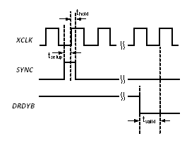 Figure 19. Single Shot Sync Setup/Hold Time
See Figure 20 for details regarding the Single Shot Flow Chart.
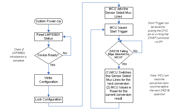 Figure 20. Single Shot Flow Chart
8.4.2 Continuous Mode
In Continuous mode the LMP93601 only requires a single Start Trigger to start. The Start Trigger can start either by a SYNC or a Start command via the SPI (SYNC is recommended). After the LOCK bit is set, the external MCU should wait 3 XCLK cycles before it sends a start trigger. This allows the internal synchronizer enough time to synchronize the SPI write of the LOCK bit into the XCLK domain. This assumes the analog has already settled (else allow ~100 µs to go from standby to conversion mode).
It will convert all enabled channels without requiring another Start Trigger. Figure 21 shows the Continuous Mode Flow Chart.
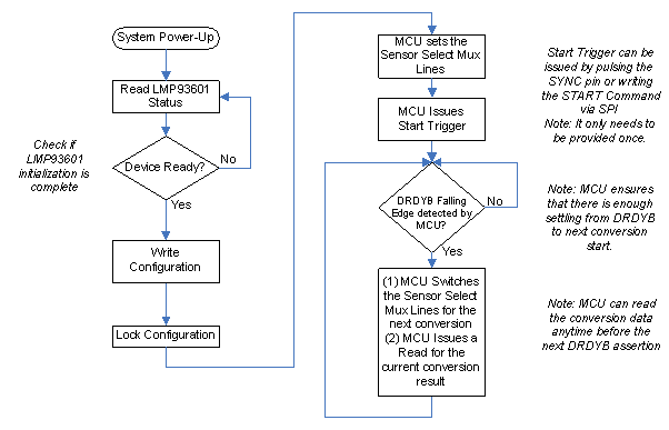 Figure 21. Continuous Mode Flow Chart
8.5 Programming
8.5.1 Window to Capture Data and Status
SPI Protocols can be asynchronous to XCLK. Data and status read can only happen between the consecutive DRDYB falling edges. For example, after DRDYB is asserted by the LMP93601, the MCU has to finish reading all data before DRDYB is asserted again.
For best performance in continuous acquisition mode, it is recommended to read the data within 70 µs after DRDYB is asserted in order to keep the SPI activity during conversion to a minimum.
NOTE
The de-assertion of DRDYB happens after a data read command is received.
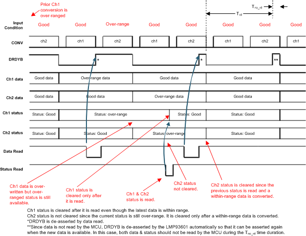 Figure 22. Channel Data Transfer Timing Diagram
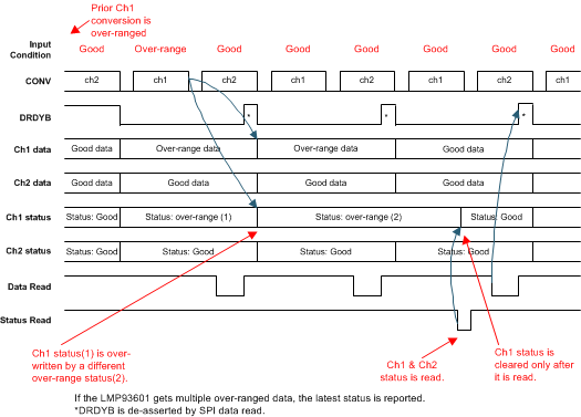 Figure 23. Channel Data Transfer Timing Diagram
8.5.2 Single Byte Access
WRITE: A single byte write access is a total of 16 SCLK periods during CSB assertion. Incoming data is captured on the rising edge of the SCLK. A command byte consists of an R/W bit and a 7-bit address field and R/W = 0 for write protocols.
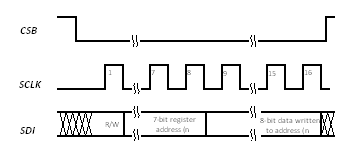 Figure 24. Single Byte Write Access
READ: Similar to a write, the LMP93601 captures incoming data on the SCLK rising edge. After the 8th rising edge, the LMP93601 output data is sourced on the SCLK falling edge and the MCU should capture it on the rising edge. R/W = 1 for read protocols.
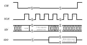 Figure 25. Single Byte Read Access
8.6 Register Maps
Table 6. LMP93601 Internal Registers
| ADDR [6:0] |
Name | # of Bits | Type | Default | Description | Locked when conversion is enabled? |
|---|---|---|---|---|---|---|
| 0x00 | Lock | 1 | R/W(1) | ‘h00 | [0] | n/a(4) |
| 0: configuration bits are writeable (default) | ||||||
| 1: configuration bits are read-only (that is, locked) unless noted. | ||||||
| [7:1] always 0 | ||||||
| 0x01 | Config1 | 4 | R/W(1) | ‘h00 | [7] continuous/single shot: | Y |
| 0: Continuous – the part will convert all enabled channels sequentially in a round-robin manner. After all channels are converted, it will repeat the round-robin. (default) | ||||||
| 1: Single-Shot - the part will convert all enabled channels once in a round-robin manner after receiving a start-trigger (SYNC pulse preferred). It will wait for the next trigger before converting all enabled channels again. | ||||||
| [2:0] Channel enable | ||||||
| Channel enable configuration for the 3 channels (Ch1-3): | ||||||
| 3’b000: Only Ch1 is enabled(default) | ||||||
| 3’b001: Only Ch2 is enabled | ||||||
| 3’b010: Only Ch3 is enabled | ||||||
| 3’b011: Only Ch1 & Ch2 enabled | ||||||
| 3’b100: Ch1, 2, & 3 enabled | ||||||
| 3’b101, 3’b110, 3’b111: Reserved | ||||||
| [6:3]: always 0 | ||||||
| 0x02 | Config2 | 3 | R/W(1) | ’h82 | [7] Reference Output Enables for VCM | Y |
| 0: Disable the corresponding VCM output | ||||||
| 1: Enable the corresponding VCM output | ||||||
| (default) | ||||||
| VCM = AVDD/3 | ||||||
| [1:0] SPS select | ||||||
| Global setting for all enabled channels | ||||||
| 2’b00: 265 sps | ||||||
| 2’b01: 530 sps | ||||||
| 2’b10: 1057 sps(default) | ||||||
| 2’b11: 1326 sps | ||||||
| [6:2] always 0 | ||||||
| 0x03 | Config3 | 5 | R/W(1) | ’h52 | PGA settings for differential channels. All channels will always have the same setting. | Y |
| [6:4] Digital | ||||||
| 3’b000: 1 | ||||||
| 3’b001: 2 | ||||||
| 3’b010: 4 | ||||||
| 3’b011: 8 | ||||||
| 3’b100: 16 | ||||||
| 3’b101: 32(default) | ||||||
| 3’b110-111: Reserved | ||||||
| [1:0] Analog | ||||||
| 2’b00: 16 | ||||||
| 2’b01: 32 | ||||||
| 2’b10: 64 (default) | ||||||
| 2’b11: 128 | ||||||
| [7], [3:2] always 0 | ||||||
| [2] , Bypass PGA, bit [1:0] would be ignored. See for more details |
||||||
| 0x04 | Config4 | 1 | R/W(1) | ‘h00 | [0] Power Mode | Y |
| 0: Standby (default) | ||||||
| 1: Conversion Mode (user still has to write the lock bit and then provide a start-trigger before conversion starts) | ||||||
| [7:1] always 0 | ||||||
| 0x05 | Alarm mask | 3 | R/W(1) | ‘h00 | [7] Brownout Mask | Y |
| 0: when brown-out is detected, all enabled channels’ conversion result will be 0x7FFF (default) | ||||||
| 1: when brown-out is detected, the conversion result is not affected. | ||||||
| [6]: Digital Gain Over range Mask | ||||||
| 0: when digital gain over-range is detected for a channel, its conversion result will be 0x7FFF (default) | ||||||
| 1: when digital gain over-range is detected, conversion result is not affected. | ||||||
| [0] PGA over-range Mask | ||||||
| 0: when any of the PGA over-range is detected for a channel, its conversion result will be 0x7FFF (default) | ||||||
| 1: when any of the PGA over-range is detected, conversion result is not affected | ||||||
| [5:1] always 0 | ||||||
| 0x06 | sdo_cfg | 1 | R/W(1) | ‘h00 | [0] SDO always driven mode | N |
| 0: SDO only driven during the read back frames of a SPI read, all other time, SDO is in Hi-Z (Default) | ||||||
| 1: SDO always driven mode: SDO driven high by LMP93601 except during the read back frame of a SPI read | ||||||
| [7:1] always 0 | ||||||
| 0x07 | Soft reset | 1 | R/W(1) | ‘h00 | [0]: Soft reset | N |
| 0: normal (Default) | ||||||
| 1: Reset all registers hence part will be in default condition | ||||||
| To reset via SPI, one should write first a 1 to this bit and then a 0. | ||||||
| [7:1] always 0 | ||||||
| 0x0f | START | 1 | WO(3) | n/a(4) | [7] Start | Only writeable if LOCK is 1 |
| This is a write-only location. If written, it will act as the trigger to start the conversion sequence. | ||||||
| In continuous mode, the round robin is triggered by a write to this register. The round robin will be repeated so only 1 write is needed. | ||||||
| In Single-Shot mode, the round robin is triggered by a write to this register and all enabled channels will be converted once. The chip will wait for the next write to the START register before starting the next round robin conversion. | ||||||
|
NOTE: For accurate timing control, SYNC pulse as a start-trigger is preferred since it is synchronous to the XCLK domain. |
||||||
| [6:0] always 0 | ||||||
|
NOTE The following status register addresses are mapped in ascending order for easy read-back. |
||||||
| 0x10 | general Status | 1 | RO(2) | ‘h00 | [0]: when this bit is high, the LMP93601 is ready to be programmed. | n/a(4) |
| 0x11 | Status1 | 8 | RO(2) | n/a(4) | [7:0]: Status for CH1: [0] - Digital gain overrange [1] - PGA positive output low [2] - PGA negative output low [3] - PGA positive output high [4] - PGA negative output high [5] - PGA differential output high [6] - Sign of PGA out. This alone does not trigger 7FFF error code. [7] Brown out |
n/a(4) |
| 0x12 | Status2 | 8 | RO(2) | n/a(4) | [7:0] Status for CH2: | n/a(4) |
| same bit map as CH1 status (above) | ||||||
| 0x13 | Status3 | 8 | RO(2) | n/a(4) | [7:0] Status for CH3: | n/a(4) |
| same bit map as CH1 status (above) | ||||||
| Channel Results: When over-range is detected, the corresponding channel result will read back 0x7FFF, unless it is masked. When brown-out is detected, the converted channel result will read back 0x7FFF, unless it is masked. |
||||||
| NOTE The following channel result register addresses are mapped in ascending order for easy read-back. | ||||||
| 0x20 | CH1 LSB | 8 | RO(2) | n/a(4) | CH1 Result[7:0] | n/a(4) |
| 0x21 | CH1 MSB | 8 | RO(2) | n/a(4) | CH1 Result[15:8] | n/a(4) |
| 0x22 | CH2 LSB | 8 | RO(2) | n/a(4) | CH2 Result[7:0] | n/a(4) |
| 0x23 | CH2 MSB | 8 | RO(2) | n/a(4) | CH2 Result[15:8] | n/a(4) |
| 0x24 | CH3 LSB | 8 | RO(2) | n/a(4) | CH3 Result[7:0] | n/a(4) |
| 0x25 | CH3 MSB | 8 | RO(2) | n/a(4) | CH3 Result[15:8] | n/a(4) |
| 0x7E | Chip ID | 8 | RO(2) | 8’h73 | LMP93601 chip ID | n/a(4) |
| 0x7F | Revision ID | 8 | RO(2) | 8’h00 | LMP93601 Revision ID | n/a(4) |
8.7 Multi Byte Access (Auto Increment) Mode
This interface will support address auto-increment feature. An access cycle may be extended to multiple registers simply by keeping the CSB asserted beyond the stated 16 clocks of the standard 16-bit protocol. In this mode, CSB must be asserted during 8*(1+N) clock cycles of SCLK, where N is the number of bytes to write or read during the access cycle. The auto-incrementing address mode is useful to access a block of registers of incrementing addresses.
WRITE: Example: if 2 bytes of data are sent by the MCU to the LMP93601, both addresses (n) and (n+1) will be written at the 16th and 24th rising edges of SCLK respectively. Similarly, if another 8 bits of data is sent, they will be written in the next address location.
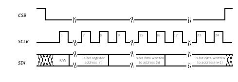 Figure 26. Example Multi Byte Write Access
READ: Example: if a read address is sent from the MCU to the LMP93601, the LMP93601 will first output the data at location (n). If another 8 SCLKs are sent, the data at location (n+1) will be output. Similarly, the LMP93601 will continue to send the data at the next address location until CSB is de-asserted.
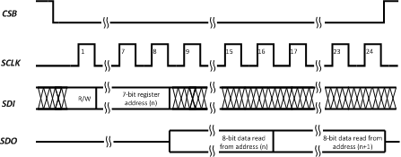 Figure 27. Example Multi Byte Read Access
NOTE
If a read (or write) is not 8*(1+N) clock cycles, the last byte will not be read or written. For example if 20 clocks were used, only the 1st data byte is being written, not the 2nd one.
8.8 Multi-Channel Data Read
CH1, CH2 and CH3 results can be read by a single SPI transaction in Little Endian Format:
- Byte Level: Ch1[7:0], Ch1[15:8], Ch2[7:0], Ch2[15:8], Ch3[7:0], Ch3[15:8]…..
- Bit Level: Ch1[7], [6], [5], [4], [3], [2], [1], [0], [15], [14], [13], [12]. [11], [10], [9], [8], Ch2[7]……..
The overhead is a single byte of command which consists of a READ bit and a 7-bit address field.
NOTE
ADC rate is 1326 SPS (max). If all 3 channels are enabled, the conversion rate for each channel is 1326 SPS/3 = 426SPS.
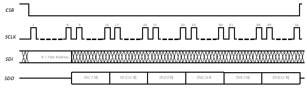 Figure 28. Example Multi Channel Read Access