ZHCSC60A March 2014 – September 2014 LMP93601
PRODUCTION DATA.
- 1 特性
- 2 应用范围
- 3 说明
- 4 简化热电堆阵列系统图
- 5 修订历史记录
- 6 Pin Configuration and Functions
- 7 Specifications
-
8 Detailed Description
- 8.1 Overview
- 8.2 Functional Block Diagram
- 8.3
Feature Description
- 8.3.1 Data Format
- 8.3.2 Transfer Function
- 8.3.3 Input Routing Mux
- 8.3.4 Programmable Gain Amplifier
- 8.3.5 PGA Bypass Mode
- 8.3.6 Over-Range Detection
- 8.3.7 Analog-To-Digital Converter (ADC)
- 8.3.8 Programmable Digital Filters
- 8.3.9 Common Mode Voltage Generator
- 8.3.10 Low Drop-Out Regulator (LDO)
- 8.3.11 External Clock
- 8.3.12 Operating Modes
- 8.3.13 Data Ready Function (DRDYB)
- 8.3.14 Synchronous Serial Peripheral Interface (SPI)
- 8.3.15 Power Management Mode; Standby, Conversion and Shutdown
- 8.3.16 Power-On Sequence and Reset (POR) Function
- 8.3.17 Brown-Out Detection Function
- 8.3.18 Reset Function
- 8.4 Device Functional Modes
- 8.5 Programming
- 8.6 Register Maps
- 8.7 Multi Byte Access (Auto Increment) Mode
- 8.8 Multi-Channel Data Read
- 9 Application and Implementation
- 10Power Supply Recommendations
- 11Layout
- 12器件和文档支持
- 13机械封装和可订购信息
7 Specifications
7.1 Absolute Maximum Ratings
over operating free-air temperature range (unless otherwise noted) (1)| MIN | MAX | UNIT | ||
|---|---|---|---|---|
| Analog Supply Voltage, AVDD | -0.3 | 6.0 | V | |
| Digital Supply Range, IOVDD; ( IOVDD must always be lower than or equal to AVDD supply) | -0.3 | 6.0 | V | |
| Voltage between any two analog pins | 6.0 | V | ||
| Voltage between any two digital pins | 6.0 | V | ||
| Voltage between XCAP2 and any GND (A, D or IO) | 2.2 | V | ||
| Input current at any pin | -5.0 | +5.0 | mA | |
| Junction Temperature | 125 | °C | ||
(1) The input negative-voltage and output voltage ratings may be exceeded if the input and output current ratings are observed.
7.2 Handling Ratings
| MIN | MAX | UNIT | |||
|---|---|---|---|---|---|
| Tstg | Storage temperature range | 150 | °C | ||
| V(ESD) | Electrostatic discharge | Human body model (HBM), per ANSI/ESDA/JEDEC JS-001, all pins(1) | 2000 K | V | |
| Charged device model (CDM), per JEDEC specification JESD22-C101, all pins(2) | 500 | ||||
(1) JEDEC document JEP155 states that 2000 -V HBM allows safe manufacturing with a standard ESD control process.
(2) JEDEC document JEP157 states that 500-V CDM allows safe manufacturing with a standard ESD control process.
7.3 Recommended Operating Conditions
| MIN | MAX | UNIT | ||
|---|---|---|---|---|
| Analog Supply Voltage, AVDD | 2.7 | 5.5 | V | |
| Fclk | 3.6 | 4.4 | MHz | |
| Digital Supply Voltage, IOVDD | 2.7 | AVDD | V | |
| Supply Ground | AGND = DGND = IOGND | |||
| Temperature range | -25 | 85 | °C | |
7.4 Thermal Information
| SYMBOL | THERMAL METRIC | WQFN 24 PINS |
UNIT |
|---|---|---|---|
| ΘJA | Thermal resistance, junction to ambient | 37.9 | °C/W |
| ΘJC | Thermal resistance, junction to case | 4.8 | °C/W |
| ΨJB | Thermal resistance, junction to board | 19.4 | °C/W |
7.5 Electrical Characteristics
Typical conditions: TA=+25⁰C, AVDD=IOVDD=3.3 V, INP1/INN1 enabled with VICM=AVDD/3. PGA gain=64, PGA over-range masked, digital gain=1. SPS select=1057 SPS. fXCLK=4.00 MHz. Conversion power mode. XCAP1=1 uF. XCAP2=0.1 uF.| SYMBOL | PARAMETER | TEST CONDITION | MIN | TYP | MAX | UNIT |
|---|---|---|---|---|---|---|
| INPUTS | ||||||
| XTLK | Crosstalk across input channels | Channel1 enabled with a 100 kΩ resistor as input, channel 2 disabled with 1 V peak-peak , 100 Hz signal as input. | 80 | dB | ||
| Zin | Differential input impedance | 10//7 | MΩ//pF (4) | |||
| Common mode input impedance | 100//4.5 | MΩ//pF(4) | ||||
| IB | Input bias current | -1.3 | nA | |||
| Ios | Input offset current on differential channels | Maximum of INP1-INN1, .., INP3-INN3 | -200 | pA | ||
| TCIos | Input offset current drift on differential channels | Maximum of INP1-INN1, .., INP3-INN3 | -0.5 | pA/⁰C | ||
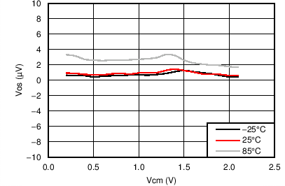
| Vos | Input referred offset voltage | Input short on chip, PGA 64 DG =1, CH1 | -15 | 1 | +15 | uV(5) |
| TCVos | Input referred offset drift with temperature | Input short on chip | 50 | nV/⁰C | ||
| Vdiff | Input differential range for AVDD≥3V | Programmable gain settings =16; ± 3% | -64 | +64 | mV | |
| Programmable gain settings =32; ± 3% | -32 | +32 | ||||
| Programmable gain settings =64; ± 3% | -16 | +16 | ||||
| Programmable gain settings = 128; ± 3% | ± 8 | |||||
| PGA bypass | ±1 | V | ||||
| VICM | Input common mode range. | PGA = 64 V/V; CMRR ≥ 80 dB | 0.3 | AVDD-1.4 | V(2) | |
| PGA = 64 V/V ; CMRR ≥ 72 dB -25 C to 85 C |
0.4 | AVDD-1.45 | ||||
| BW | Channel bandwidth | See Figure 16 | Hz | |||
| ODR | Output data rate | 265 | SPS | |||
| 530 | ||||||
| 1057 | ||||||
| 1326 | ||||||
| PGA | Programmable gain settings | 16, 32 , 64 and 128 | V/V | |||
| Bypass mode | 1 | V/V | ||||
| Digital Gain | Programmable gain settings | 1, 2, 4, 8, 16 and 32 | V/V | |||
| Total AFE Gain | Programmable gain settings (analog and digital) | 16 - 4096 | V/V | |||
| Gain steps | 2 x | |||||
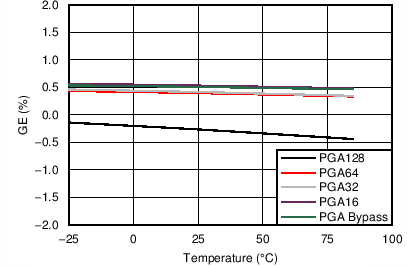
| GE | Gain error | 0.3 % | ||||
| PGA bypassed | -0.3 % | |||||
| GE drift with temperature | -9 | ppm/⁰C | ||||
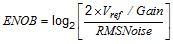
| ENOB(1) | Effective number of bits | 15.3 | Bits | |||
| THD | Total harmonic distortion (Linearity) | 100 Hz, 50 mVpp differential input, PGA 16 V/V | 91 | dB | ||
| Noise | RMS noise in a 1 kHz BW | PGA = 64 V/V | 0.67(6) | uVrms | ||
| 1/ƒ noise corner | 1 | Hz | ||||
| CMRR | Common mode rejection ratio (at DC) | VICM = 0.3 to AVDD-1.4 V | 80 | 127 | dB(2) | |
| VICM = 0.4 to AVDD-1.45 V, over operating temperature range -25 C to 85 C |
72 | 127 | ||||
| PSRR | Power supply rejection ratio (at DC) | Supply ; 2.7 to 5.5 V | 80 | 120 | dB(2) | |
| Supply ; 2.7 to 5.5 V, over operating temperature range -25 C to 85 C |
72 | 120 | ||||
| EMIRR | EMI rejection ratio | VRF = 100 mVPP | dB | |||
| f=400 MHz | 86 | |||||
| f=900 MHz | 87 | |||||
| f=1800 MHz | 85 | |||||
| f=2400 MHz | 84 | |||||
| VCM | ||||||
| V VCM | Output voltage | AVDD/3 | V | |||
| Tstrp VCM | Startup time | To within 90% of final value | 10 | ms | ||
| Acc VCM | Accuracy | 0.2 | % | |||
| TC VCM | Drift over temperature | 0.5 | ppm/⁰C | |||
| I VCM | Output current | 0.5 | mA | |||
| Load regulation | 0 to 200uA | 4 | 15 | mV | ||
| Zload VCM | Load range | 2.2//100 | MΩ//nF | |||
| SLAVE SPI INTERFACE | ||||||
| Clock frequency | 1 | 20 | MHz | |||
| DIGITAL INPUT/OUTPUT CHARACTERISTICS | ||||||
| VIH | Logical “1” Input Voltage | 0.7x IOVDD |
V | |||
| VIL | Logical “0” Input Voltage | 0.3x IOVDD |
V | |||
| VOH | Isource=300uA | IOVDD- 0.150 |
||||
| VOL | Isink=300uA | IOGND +0.150 |
||||
| POWER SUPPLY | ||||||
| AVDD | Analog supply voltage range | 2.7 | 5.5 | V | ||
| IOVDD | Digital supply voltage range | AVDD ≥ IOVDD | AVDD | V(3) | ||
| SUPPLY CURRENT | ||||||
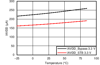
| IIOVDD | Digital on AFE | Shutdown Mode, XCLK off | 0.1 | 1 | µA | |
| Standby Mode | 1.9 | 25 | µA | |||
| Conversion Power Mode | 2.7 | 25 | µA | |||
| Conversion Power Mode, PGA bypassed |
3 | µA | ||||
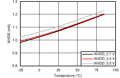
| IAVDD | Analog on AFE | Shutdown Mode, XCLK off | 0.1 | 1 | µA | |
| Standby Mode | 175 | 250 | µA | |||
| Conversion Power Mode | 1.1 | 1.6 | mA | |||
| Conversion Power Mode, 230 μA PGA bypassed | 230 | µA | ||||
| TEMPERATURE RANGE | ||||||
| Operating | –25 | 85 | °C | |||
(1) ENOB is a DC ENOB spec, not the dynamic ENOB that is measured using FFT and SINAD:
(2) Temperature limits are ensured by statistical analysis or design
(3) IOVDD always ≤ AVDD and IOVDD minimum is 2.7 V
(4) Value from simulation
(5) The input referred offset is measure by an on-chip short.
(6) See Table 1 for detailed noise performance
7.6 Timing Requirements
Under typical conditions with maximum total load capacitance 10 pF.| MIN | TYP | MAX | UNIT | ||
|---|---|---|---|---|---|
| tPH | High Period, SCLK | 25 | ns | ||
| tPL | Low Period, SCLK | 25 | ns | ||
| tSU | SDI input setup time | 10 | ns | ||
| tH | SDI input hold time | 10 | ns | ||
| tOD | SDO output hold time | 13.5 | ns | ||
| tCSS | CSB setup time | 25 | ns | ||
| tCSH | CSB hold time | 25 | ns | ||
| tIAG | CSB high time | 50 | ns |
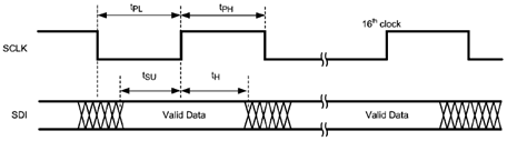 Figure 1. SPI Write Timing Diagram
 Figure 2. SPI Read Timing Diagram
7.7 Noise Performance
Table 1. Noise In µVRMS at AVDD= 3.3 V, AGND = 0 V, and Internal Reference = 2.4 VRMS
| ODR (SPS) | PGA Gain (V/V) | D-Gain (V/V) | Vn (uVrms) |
|---|---|---|---|
| 265 | 16 | 1 | Below the resolution of the 16 bit SDM. |
| 2 | Below the resolution of the 16 bit SDM. |
||
| 4 | 0.661 | ||
| 8 | 0.597 | ||
| 16 | 0.578 | ||
| 32 | 0.574 | ||
| 32 | 1 | Below the resolution of the 16 bit SDM. |
|
| 2 | 0.516 | ||
| 4 | 0.396 | ||
| 8 | 0.368 | ||
| 16 | 0.361 | ||
| 32 | 0.362 | ||
| 64 | 1 | 0.556 | |
| 2 | 0.321 | ||
| 4 | 0.287 | ||
| 8 | 0.281 | ||
| 16 | 0.275 | ||
| 32 | 0.277 | ||
| 128 | 1 | 0.298 | |
| 2 | 0.254 | ||
| 4 | 0.247 | ||
| 8 | 0.242 | ||
| 16 | 0.242 | ||
| 32 | 0.240 | ||
| 530 | 16 | 1 | Below the resolution of the 16 bit SDM. |
| 2 | 0.944 | ||
| 4 | 0.888 | ||
| 8 | 0.831 | ||
| 16 | 0.810 | ||
| 32 | 0.816 | ||
| 32 | 1 | 0.509 | |
| 2 | 0.609 | ||
| 4 | 0.543 | ||
| 8 | 0.517 | ||
| 16 | 0.521 | ||
| 32 | 0.511 | ||
| 64 | 1 | 0.569 | |
| 2 | 0.421 | ||
| 4 | 0.397 | ||
| 8 | 0.396 | ||
| 16 | 0.397 | ||
| 32 | 0.395 | ||
| 128 | 1 | 0.377 | |
| 2 | 0.348 | ||
| 4 | 0.340 | ||
| 8 | 0.341 | ||
| 16 | 0.340 | ||
| 32 | 0.339 | ||
| 1057 | 16 | 1 | 1.565 |
| 2 | 1.517 | ||
| 4 | 1.410 | ||
| 8 | 1.409 | ||
| 16 | 1.398 | ||
| 32 | 1.401 | ||
| 32 | 1 | 0.932 | |
| 2 | 0.903 | ||
| 4 | 0.834 | ||
| 8 | 0.839 | ||
| 16 | 0.829 | ||
| 32 | 0.824 | ||
| 64 | 1 | 0.667 | |
| 2 | 0.596 | ||
| 4 | 0.580 | ||
| 8 | 0.580 | ||
| 16 | 0.579 | ||
| 32 | 0.574 | ||
| 128 | 1 | 0.501 | |
| 2 | 0.481 | ||
| 4 | 0.476 | ||
| 8 | 0.476 | ||
| 16 | 0.473 | ||
| 32 | 0.470 | ||
| 1326 | 16 | 1 | 2.331 |
| 2 | 1.743 | ||
| 4 | 1.743 | ||
| 8 | 1.665 | ||
| 16 | 1.648 | ||
| 32 | 1.681 | ||
| 32 | 1 | 1.189 | |
| 2 | 0.975 | ||
| 4 | 0.981 | ||
| 8 | 0.954 | ||
| 16 | 0.941 | ||
| 32 | 0.937 | ||
| 64 | 1 | 0.733 | |
| 2 | 0.677 | ||
| 4 | 0.670 | ||
| 8 | 0.667 | ||
| 16 | 0.660 | ||
| 32 | 0.663 | ||
| 128 | 1 | 0.575 | |
| 2 | 0.546 | ||
| 4 | 0.541 | ||
| 8 | 0.537 | ||
| 16 | 0.540 | ||
| 32 | 0.538 |
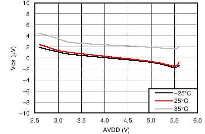
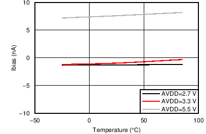
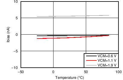
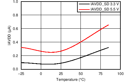
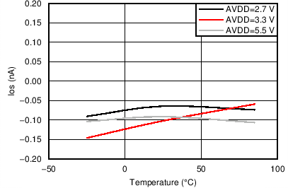
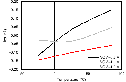
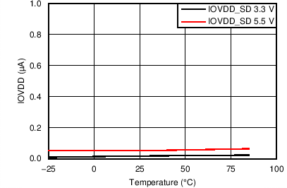
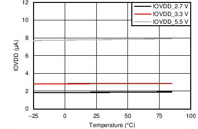
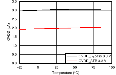
7.8 Typical Characteristics