ZHCSDV7 July 2015 LM57-Q1
PRODUCTION DATA.
- 1 特性
- 2 应用范围
- 3 说明
- 4 Device Comparison Table
- 5 Pin Configuration and Functions
- 6 Specifications
-
7 Detailed Description
- 7.1 Overview
- 7.2 Functional Block Diagram
- 7.3 Feature Description
- 7.4 Device Functional Modes
- 8 Application and Implementation
- 9 Power Supply Recommendations
- 10Layout
- 11器件和文档支持
- 12机械、封装和可订购信息
6 Specifications
6.1 Absolute Maximum Ratings
over operating free-air temperature range (unless otherwise noted) (1)(2)| MIN | MAX | UNIT | ||
|---|---|---|---|---|
| Supply voltage | −0.3 | 6 | V | |
| Voltage at TOVER | −0.3 | 6 | V | |
| Voltage at TOVER , VTEMP, TRIP-TEST, SENSE1, and SENSE2 | −0.3 | (VDD + 0.3 V) | V | |
| Current at any pin | 5 | mA | ||
| Storage temperature for LM57FSPWQ1 and LM57TSPWQ1 | −65 | 175 | °C | |
| Storage temperature for all LM57-Q1 except LM57FSPWQ1 and LM57TSPWQ1 | −65 | 150 | °C | |
(1) Stresses beyond those listed under Absolute Maximum Ratings may cause permanent damage to the device. These are stress ratings only, which do not imply functional operation of the device at these or any other conditions beyond those indicated under Recommended Operating Conditions. Exposure to absolute-maximum-rated conditions for extended periods may affect device reliability.
(2) Soldering process must comply with Reflow Temperature Profile specifications. Refer to www.ti.com/packaging.
6.2 ESD Ratings
| VALUE | UNIT | |||
|---|---|---|---|---|
| V(ESD) | Electrostatic discharge | Human-body model (HBM), per AEC Q100-002 (1) | ±2000 | V |
| Charged-device model (CDM), per AEC Q100-011 | ±750 | |||
(1) AEC Q100-002 indicates that HBM stressing shall be in accordance with the ANSI/ESDA/JEDEC JS-001 specification.
6.3 Recommended Operating Conditions
| MIN | NOM | MAX | UNIT | ||
|---|---|---|---|---|---|
| FOR ALL PARTS GRADE 0 AND GRADE 1 EXCEPT GRADE 0 EXTENDED (LM57FSPWQ1 and LM57TSPWQ1) | |||||
| Supply voltage | 2.4 | 5.5 | V | ||
| Free air temperature range (TMIN ≤ TA ≤ TMAX) | LM57FEPWQ1, and LM57TEPWQ1 | −50 | 150 | °C | |
| LM57FQPWQ1, LM57TQPWQ1 | -50 | 125 | °C | ||
| GRADE 0 EXTENDED (LM57FSPWQ1 AND LM57TSPWQ1) | |||||
| Supply voltage | 2.4 | 5.5 | V | ||
| Free air temperature range (TMIN ≤ TA ≤ TMAX) | Temperature Profile for LM57-Q1 Automotive Grade 0 Extended High Temperature Operational Life Test (HTOL) - Hours of Operation: (1) | −50 | 170 | °C | |
| 1700 hours at TJ = TC = 160°C | |||||
| 10 hours at TJ = TC = 170°C | |||||
(1) Except for HTOL testing, which was conducted as described, all other testing was to AEC-Q100 Grade 0 flow. Full details on reliability testing are available upon request.
6.4 Thermal Information
| THERMAL METRIC (1) | LM57-Q1 | UNIT | |
|---|---|---|---|
| PW (TSSOP) | |||
| 8 PINS | |||
| RθJA | Junction-to-ambient thermal resistance | 183 | °C/W |
| RθJC(top) | Junction-to-case (top) thermal resistance | 66 | °C/W |
| RθJB | Junction-to-board thermal resistance | 111 | °C/W |
| ψJT | Junction-to-top characterization parameter | 8 | °C/W |
| ψJB | Junction-to-board characterization parameter | 110 | °C/W |
| RθJC(bot) | Junction-to-case (bottom) thermal resistance | — | °C/W |
(1) For more information about traditional and new thermal metrics, see the Semiconductor and IC Package Thermal Metrics application report, SPRA953.
6.5 Electrical Characteristics
Unless otherwise noted, these specifications apply for VDD = 2.4 to 5.5 V and over free air temperature range. These limits do not include DC load regulation. These stated accuracy limits are with reference to the values in Table 1.| PARAMETER | TEST CONDITIONS | MIN | TYP | MAX | UNIT | |||
|---|---|---|---|---|---|---|---|---|
| TRIP POINT ACCURACY FOR ALL LM57-Q1 EXCEPT LM57FSPWQ1 AND LM57TSPWQ1 | ||||||||
| Trip Point Accuracy (Includes 1% set-resistor tolerance) |
J2 | TA = −41°C to 52°C | VDD = 2.4 V to 5.5 V | ±2.3 | °C | |||
| J3 | TA = 52°C to 97°C | VDD = 2.4 V to 5.5 V | ±2.3 | °C | ||||
| J4 | TA = 97°C to 119°C | VDD = 2.4 V to 5.5 V | ±2.3 | °C | ||||
| J5 | TA = 119°C to free air temperature max | VDD = 2.4 V to 5.5 V | ±2.3 | °C | ||||
| TRIP POINT ACCURACY FOR LM57-Q1 AUTOMOTIVE GRADE 0 EXTENDED (LM57FSPWQ1 and LM57TSPWQ1) | ||||||||
| Trip point accuracy (Includes 1% set-resistor tolerance) |
J2 | TA = −41°C to 52°C | VDD = 2.4 V to 5.5 V | ±2.3 | °C | |||
| J3 | TA = 52°C to 97°C | |||||||
| J4 | TA = 97°C to 119°C | |||||||
| J5 | TA = 119°C to 160°C | |||||||
| J5 | TA = 150°C to 160°C | VDD = 2.4 V to 5.5 V | ±2.5 | |||||
| VTEMP ANALOG TEMPERATURE SENSOR OUTPUT ACCURACY FOR ALL LM57-Q1 EXCEPT LM57FSPWQ1 and LM57TSPWQ1 | ||||||||
| VTEMP Accuracy (These stated accuracy limits are with reference to the values in Table 1, LM57-Q1 VTEMP Temperature-to-Voltage.) |
J2 | TA = −50°C to free air temperature max | VDD = 2.4 V to 5.5 V | ±1.3 | °C | |||
| J3 | TA = −50°C to free air temperature max | VDD = 2.4 V to 5.5 V | ±1.3 | °C | ||||
| J4 | TA = 20°C to 50°C | VDD = 2.4 V to 5.5 V | ±1.3 | °C | ||||
| TA = 0°C to free air temperature max | VDD = 2.7 V to 5.5 V | ±1.3 | ||||||
| TA = −50°C to 0°C | VDD = 3.1 V to 5.5 V | ±1.3 | ||||||
| J5 | TA = 60°C to free air temperature max | VDD = 2.4 V to 5.5 V | ±1.3 | °C | ||||
| TA = 20°C to 50°C | VDD = 2.9 V to 5.5 V | ±1.3 | ||||||
| TA = 0°C to free air temperature max | VDD = 3.2 V to 5.5 V | ±1.3 | ||||||
| TA = −50°C to 0°C | VDD = 4 V to 5.5 V | ±1.3 | ||||||
| VTEMP ANALOG TEMPERATURE SENSOR OUTPUT ACCURACY FOR LM57-Q1 AUTOMOTIVE GRADE 0 EXTENDED (LM57FSPWQ1 and LM57TSPWQ1) | ||||||||
| VTEMP accuracy (These stated accuracy limits are with reference to the values in Table 1, LM57-Q1 VTEMP temperature-to-voltage.) |
J2 | TA = 150°C to 160°C | VDD = 2.4 V to 5.5 V | ±1.5 | °C | |||
| TA = –50°C to 150°C | ±1.3 | |||||||
| J3 | TA = 150°C to 160°C | VDD = 2.4 V to 5.5 V | ±1.5 | °C | ||||
| TA = –50°C to 150°C | ±1.3 | |||||||
| J4 | TA = 20°C to 50°C | VDD = 2.4 V to 5.5 V | ±1.3 | °C | ||||
| TA = 0°C to 150°C | VDD = 2.7 V to 5.5 V | ±1.3 | ||||||
| TA = 150°C to 160°C | ±1.5 | |||||||
| TA = –50°C to 0°C | VDD = 3.1 V to 5.5 V | ±1.3 | ||||||
| J5 | TA = 150°C to 160°C | VDD = 2.4 V to 5.5 V | ±1.5 | °C | ||||
| TA = 60°C to 150°C | ±1.3 | |||||||
| TA = 20°C to 50°C | VDD = 2.9 V to 5.5 V | ±1.3 | ||||||
| TA = 0°C to 150°C | VDD = 3.2 V to 5.5 V | ±1.3 | ||||||
| TA = –50°C to 0°C | VDD = 4 V to 5.5 V | ±1.3 | ||||||
| OTHER TEMPERATURE SENSOR SPECIFICATIONS | ||||||||
| VTEMP sensor gain | J2: −50°C to 52°C | −5.166 | mV/°C | |||||
| J3: 52°C to 97°C | −7.752 | |||||||
| J4: 97°C to 119°C | −10.339 | |||||||
| J5: 119°C to 160°C | −12.924 | |||||||
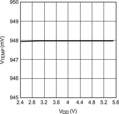
| Line regulation DC: supply-to-VTEMP(1) | Temp = 90°C | 0.18 | mV | |||||
| 58 | μV/V | |||||||
| −84 | dB | |||||||
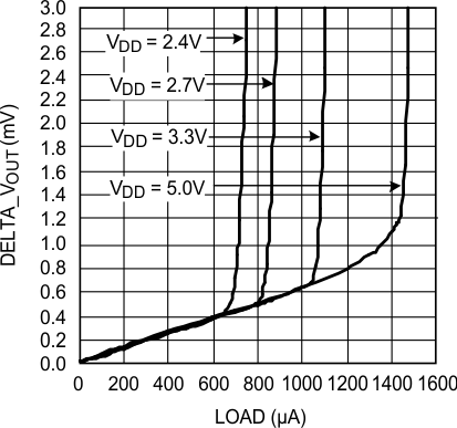
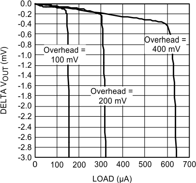
| Load regulation: VTEMP output (4) | Source ≤ 240 µA, (VDD – VTEMP) ≥ 200 mV; TA = −50°C to 150°C | −1 | mV | |||||
| Sink ≤ 300 µA, VTEMP ≥ 360 mV; TA = −50°C to 150°C | 1 | |||||||
| Source or sink = 100 µA; TA = −50°C to 150°C | 1 | Ω | ||||||
| Maximum Load capacitance: VTEMP output | No output series resistor required; (See VTEMP Capacitive Loads) | 1100 | pF | |||||
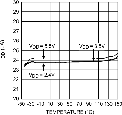
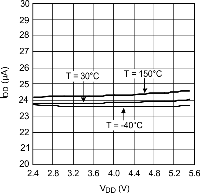
| IS | Supply current: quiescent (2) | for all LM57-Q1 for TA ≤ 150°C | 24 | 28 | µA | |||
| TA = 150°C to 160°C for LM57FSPWQ1 and LM57TSPWQ1 | 24 | 29 | µA | |||||
| TA = 170°C for LM57FSPWQ1 and LM57TSPWQ1 | 26 | µA | ||||||
| TRIP-TEST INPUT | ||||||||
| VIH | Logic 1 threshold voltage | VDD – 0.5 | V | |||||
| VIL | Logic 0 threshold voltage | 0.5 | V | |||||
| IIH | Logic 1 input current | 1.4 | 3 | µA | ||||
| IIL | Logic 0 input leakage current (3) | TA = −50°C to 150°C | 0.001 | 1 | µA | |||
| TOVER (PUSH-PULL, ACTIVE-HIGH) OUTPUT | ||||||||
| VOH | Logic 1 push-pull output voltage | Source ≤ 600 µA | VDD – 0.2 | V | ||||
| Source ≤ 1.2 mA | VDD – 0.45 | |||||||
| VOL | Logic 0 output voltage | Sink ≤ 600 µA | 0.2 | V | ||||
| Sink ≤ 1.2 mA | 0.45 | |||||||
| TOVER (OPEN-DRAIN, ACTIVE-LOW) OUTPUT | ||||||||
| VOL | Logic 0 output voltage | Sink ≤ 600 µA | 0.2 | V | ||||
| Sink ≤1.2 mA | 0.45 | |||||||
| IOH | Logic 1 output leakage current (3) | Temperature = 30°C; | 0.001 | 1 | µA | |||
| HYSTERESIS | ||||||||
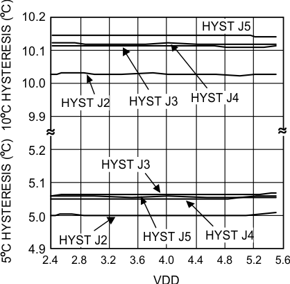
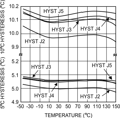
| THYST | Hysteresis temperature | 5°C hysteresis option (all LM57F for TA ≤ 150°C) | 4.7 | 5 | 5.4 | °C | ||
| 10°C hysteresis option (all LM57T for TA ≤ 150°C) | 9.6 | 10 | 10.6 | °C | ||||
| 5°C hysteresis option (LM57FSPWQ1); TA = 150°C to 160°C | 4.6 | 5 | 5.4 | °C | ||||
| 10°C hysteresis option (LM57TSPWQ1); TA = 150°C to 160°C | 9.4 | 10 | 10.6 | °C | ||||
(1) Line regulation (DC) is calculated by subtracting the output voltage at the highest supply voltage from the output voltage at the lowest supply voltage. The typical DC line regulation specification does not include the output voltage shift discussed in VTEMP Voltage Shift.
(2) Supply current refers to the quiescent current of the LM57-Q1 only and does not include any load current
(3) This current is leakage current only and is therefore highest at high temperatures. Prototype test indicate that the leakage is well below 1 μA over the full temperature range. This 1 μA specification reflects the limitations of measuring leakage at room temperature. For this reason only, the leakage current is not specified at a lower value.
(4) Source currents are flowing out of the LM57-Q1. Sink currents are flowing into the LM57-Q1. Load Regulation is calculated by measuring VTEMP at 0 μA and subtracting the value with the conditions specified.
6.6 Switching Characteristics
Unless otherwise noted, these specifications apply for VDD = 2.4 to 5.5 V over the free air temperature range.| PARAMETER | TEST CONDITIONS | MIN | TYP | MAX | UNIT | ||
|---|---|---|---|---|---|---|---|
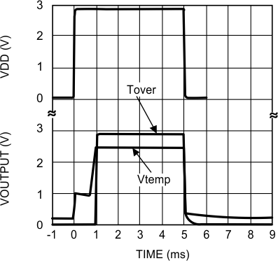
| tEN | Maximum time from power on to digital output enabled | 1.5 | ms | ||||
| tVTEMP | Maximum time from power on to analog temperature (VTEMP) valid | 1.5 | ms | ||||
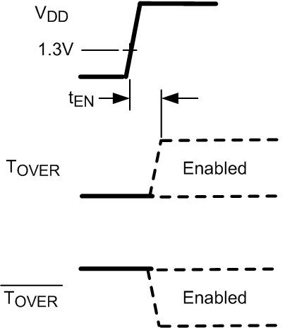 Figure 1. Definition of tEN
 Figure 2. Definition of tVTEMP
6.7 Typical Characteristics
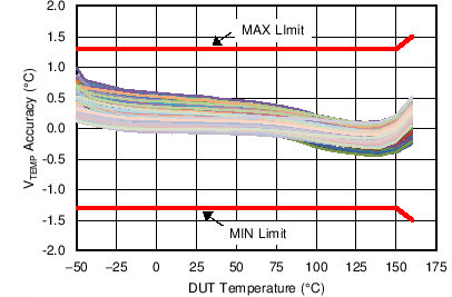
| Conditions: J2, VDD=5V |
