SLVS075J April 1989 – January 2015 LM285-1.2 , LM385-1.2 , LM385B-1.2
PRODUCTION DATA.
- 1 Features
- 2 Applications
- 3 Description
- 4 Simplified Schematic
- 5 Revision History
- 6 Pin Configuration and Functions
- 7 Specifications
- 8 Detailed Description
- 9 Application and Implementation
- 10Power Supply Recommendations
- 11Layout
- 12Device and Documentation Support
- 13Mechanical, Packaging, and Orderable Information
封装选项
请参考 PDF 数据表获取器件具体的封装图。
机械数据 (封装 | 引脚)
- D|8
- PW|8
- LP|3
散热焊盘机械数据 (封装 | 引脚)
订购信息
7 Specifications
7.1 Absolute Maximum Ratings
over operating free-air temperature range (unless otherwise noted)(1)| MIN | MAX | UNIT | |||
|---|---|---|---|---|---|
| IR | Reverse Current | 30 | mA | ||
| IF | Forward Current | 10 | mA | ||
| TJ | Operating virtual junction temperature | 150 | °C | ||
| Tstg | Storage temeprature | –65 | 150 | °C | |
(1) Stresses beyond those listed under Absolute Maximum Ratings may cause permanent damage to the device. These are stress ratings only, which do not imply functional operation of the device at these or any other conditions beyond those indicated under Recommended Operating Conditions. Exposure to absolute-maximum-rated conditions for extended periods may affect device reliability.
7.2 ESD Ratings
| VALUE | UNIT | |||
|---|---|---|---|---|
| V(ESD) | Electrostatic discharge | Human body model (HBM), per ANSI/ESDA/JEDEC JS-001, all pins(1) | ±2000 | V |
| Charged device model (CDM), per JEDEC specification JESD22-C101, all pins(2) | ±1000 | |||
(1) JEDEC document JEP155 states that 500-V HBM allows safe manufacturing with a standard ESD control process.
(2) JEDEC document JEP157 states that 250-V CDM allows safe manufacturing with a standard ESD control process.
7.3 Recommended Operating Conditions
over operating free-air temperature range (unless otherwise noted)| MIN | MAX | UNIT | |||
|---|---|---|---|---|---|
| IZZ | Reference current | 0.01 | 20 | mA | |
| TA | Operating free-air temperature | LM285-1.2 | –40 | 85 | °C |
| LM385-1.2, LM385B-1.2 | 0 | 70 | |||
7.4 Thermal Information
| THERMAL METRIC(1) | LMx85-1.2 | UNIT | ||||
|---|---|---|---|---|---|---|
| D | LP | PS | PW | |||
| 8 PINS | 3 PINS | 8 PINS | 8 PINS | |||
| RθJA | Junction-to-ambient thermal resistance | 97 | 140 | 95 | 149 | °C/W |
(1) For more information about traditional and new thermal metrics, see the IC Package Thermal Metrics application report, SPRA953.
7.5 Electrical Characteristics
over operating free-air temperature range (unless otherwise noted)| PARAMETER | TEST CONDITIONS | TA(1) | LM285-1.2 | LM385-1.2 | LM385B-1.2 | UNIT | ||||||||||
|---|---|---|---|---|---|---|---|---|---|---|---|---|---|---|---|---|
| MIN | TYP | MAX | MIN | TYP | MAX | MIN | TYP | MAX | ||||||||
| VZ | Reference voltage | IZ = I(min) to 20 mA(2) | 25°C | 1.223 | 1.235 | 1.247 | 1.21 | 1.235 | 1.26 | 1.223 | 1.235 | 1.247 | V | |||
| αVZ | Average temperature coefficient of reference voltage(3) | IZ = I(min) to 20 mA(2) | Full Range | ±20 | ±20 | ±20 | ppm/°C | |||||||||
| ΔVZ | Change in reference voltage with current | IZ = I(min) to 1 mA(2) | 25°C | 1 | 1 | 1 | mV | |||||||||
| Full Range | 1.5 | 1.5 | 1.5 | |||||||||||||
| IZ = I(min) to 20 mA | 25°C | 12 | 20 | 20 | ||||||||||||
| Full Range | 30 | 30 | 30 | |||||||||||||
| ΔVZ/Δt | Long-term change in reference voltage | IZ = 100 µA | 25°C | ±20 | ±20 | ±20 | ppm/khr | |||||||||
| IZ(min) | Minimum reference current | Full Range | 8 | 10 | 8 | 15 | 8 | 15 | µA | |||||||
| ZZ | Reference impedance | IZ = 100 µA, f = 25 Hz | 25°C | 0.2 | 0.6 | 0.4 | 1 | 0.4 | 1 | Ω | ||||||
| Full Range | 1.5 | 1.5 | 1.5 | |||||||||||||
| Vn | Broadband noise voltage | IZ = 100 µA, f = 10 Hz to 10 kHz | 25°C | 60 | 60 | 60 | µV | |||||||||
(1) Full range is −40°C to 85°C for the LM285-1.2 and 0°C to 70°C for the LM385-1.2 and LM385B-1.2.
(2) I(min) = 10 μA for the LM285-1.2 and 15 μA for the LM385-1.2 and LM385B-1.2
(3) The average temperature coefficient of reference voltage is defined as the total change in reference voltage divided by the specified temperature range.
7.6 Typical Characteristics
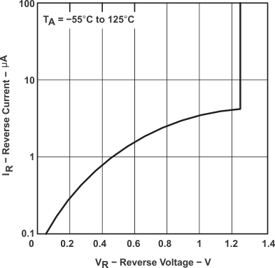 Figure 1. Reverse Current vs Reverse Voltage
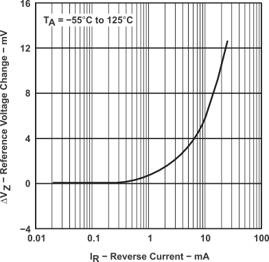 Figure 2. Reference Voltage Change vs Reverse Current
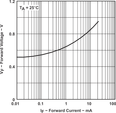 Figure 3. Forward Voltage vs Forward Current
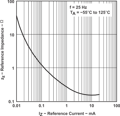 Figure 5. Reference Impedance vs Reference Current
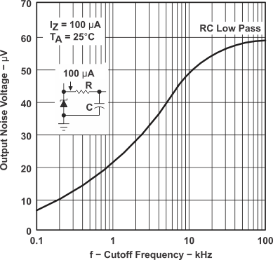 Figure 7. Output Noise Voltage vs Cutoff Frequency
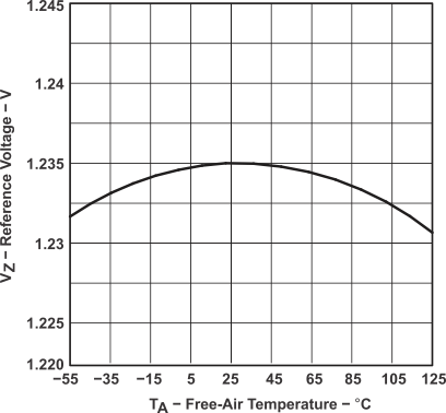 Figure 4. Reference Voltage vs Free-Air Temperature
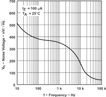 Figure 6. Noise Voltage vs Frequency