SLVS075J April 1989 – January 2015 LM285-1.2 , LM385-1.2 , LM385B-1.2
PRODUCTION DATA.
- 1 Features
- 2 Applications
- 3 Description
- 4 Simplified Schematic
- 5 Revision History
- 6 Pin Configuration and Functions
- 7 Specifications
- 8 Detailed Description
- 9 Application and Implementation
- 10Power Supply Recommendations
- 11Layout
- 12Device and Documentation Support
- 13Mechanical, Packaging, and Orderable Information
封装选项
请参考 PDF 数据表获取器件具体的封装图。
机械数据 (封装 | 引脚)
- D|8
- PW|8
- LP|3
散热焊盘机械数据 (封装 | 引脚)
订购信息
11 Layout
11.1 Layout Guidelines
Figure 12 shows an example of a PCB layout of LMx85x-1.2. Some key Vref niose considerations are:
- Connect a low-ESR, 0.1-μF (CL) ceramic bypass capacitor on the cathode pin node.
- Decouple other active devices in the system per the device specifications.
- Using a solid ground plane helps distribute heat and reduces electromagnetic interference (EMI) noise pickup.
- Place the external components as close to the device as possible. This configuration prevents parasitic errors (such as the Seebeck effect) from occurring.
- Do not run sensitive analog traces in parallel with digital traces. Avoid crossing digital and analog traces if possible and only make perpendicular crossings when absolutely necessary.
11.2 Layout Example
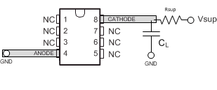 Figure 12. Layout Diagram