SLVS075J April 1989 – January 2015 LM285-1.2 , LM385-1.2 , LM385B-1.2
PRODUCTION DATA.
- 1 Features
- 2 Applications
- 3 Description
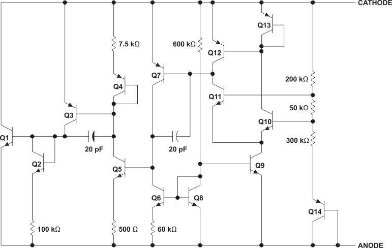
- 4 Simplified Schematic
- 5 Revision History
- 6 Pin Configuration and Functions
- 7 Specifications
- 8 Detailed Description
- 9 Application and Implementation
- 10Power Supply Recommendations
- 11Layout
- 12Device and Documentation Support
- 13Mechanical, Packaging, and Orderable Information
封装选项
请参考 PDF 数据表获取器件具体的封装图。
机械数据 (封装 | 引脚)
- D|8
- PW|8
- LP|3
散热焊盘机械数据 (封装 | 引脚)
订购信息
8 Detailed Description
8.1 Overview
The LM285-1.2, LM385-1.2, and LM385-1.2 devices are micropower, two-terminal, band-gap voltage references which operate over a 10-μA to 20-mA current range. On-chip trimming provides tight voltage tolerance. The band-gap reference for these devices has low noise and long-term stability.
The design makes these devices exceptionally tolerant of capacitive loading and, thus, easier to use in most reference applications. The wide dynamic operating temperature range accommodates varying current supplies, with excellent regulation.
The extremely low power drain of this series makes them useful for micropower circuitry. These voltage references can be used to make portable meters, regulators, or general-purpose analog circuitry, with battery life approaching shelf life.
8.2 Functional Block Diagram
8.3 Feature Description
A band gap voltage reference controls high gain amplifier and shunt pass element to maintain a nearly constant voltage between cathode and anode. Regulation occurs after a minimum current is provided to power the voltage divider and amplifier. Internal frequency compensation provides a stable loop for all capacitor loads. Floating shunt design is useful for both positive and negative regulation applications.
8.4 Device Functional Modes
LM285-1.2, LM385-1.2, and LM385-1.2 devices will operate in one mode, which is as a fixed voltage reference that cannot be adjusted.
In order for a proper Reverse Voltage to be developed, current must be sourced into the cathode of LM285. The minimum current needed for proper regulation is denoted in Electrical Characteristics as IZ,min.