ZHCSD27 October 2014 LM3648
PRODUCTION DATA.
- 1 特性
- 2 应用
- 3 说明
- 4 修订历史记录
- 5 Pin Configuration and Functions
- 6 Specifications
-
7 Detailed Description
- 7.1 Overview
- 7.2 Functional Block Diagram
- 7.3 Feature Description
- 7.4 Device Functioning Modes
- 7.5 Programming
- 7.6
Register Descriptions
- 7.6.1 Enable Register (0x01)
- 7.6.2 IVFM Register (0x02)
- 7.6.3 LED Flash Brightness Register (0x03)
- 7.6.4 LED Torch Brightness Register (0x05)
- 7.6.5 Boost Configuration Register (0x07)
- 7.6.6 Timing Configuration Register (0x08)
- 7.6.7 TEMP Register (0x09)
- 7.6.8 Flags1 Register (0x0A)
- 7.6.9 Flags2 Register (0x0B)
- 7.6.10 Device ID Register (0x0C)
- 7.6.11 Last Flash Register (0x0D)
- 8 Applications and Implementation
- 9 Power Supply Recommendations
- 10Layout
- 11器件和文档支持
- 12机械封装和可订购信息
5 Pin Configuration and Functions
DSBGA (YFF)
12 Pins
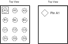
Pin Functions
| PIN | TYPE(1) | DESCRIPTION | ||
|---|---|---|---|---|
| NUMBER | NAME | |||
| A1 | GND | G | Ground | |
| A2 | IN | P | Input voltage connection. Connect IN to the input supply and bypass to GND with a 10-µF or larger ceramic capacitor. | |
| A3 | SDA | I/O | Serial data input/output in the I2C Mode on LM3648. | |
| B1 | SW | P | Drain Connection for Internal NMOS and Synchronous PMOS Switches. | |
| B2 | STROBE | I | Active high hardware flash enable. Drive STROBE high to turn on Flash pulse. Internal pulldown resistor of 300 kΩ between STROBE and GND. | |
| B3 | SCL | I | Serial clock input for LM3648. | |
| C1 | OUT | P | Step-up DC/DC CONVERTER Output. Connect a 10-µF ceramic capacitor between this terminal and GND. | |
| C2 | HWEN | I | Active high enable pin. High = Standby, Low = Shutdown/Reset. Internal pulldown resistor of 300 kΩ between HWEN and GND. | |
| C3 | TORCH/TEMP | I/P | Torch terminal input or threshold detector for NTC temperature sensing and current scale back. | |
| D1 | LED | P | High-side current source output for flash LED. Connect pin D1 to D3 externally. | |
| D2 | TX | I | Configurable dual polarity power amplifier synchronization input. Internal pulldown resistor of 300 kΩ between TX and GND. | |
| D3 | LED | P | High-side current source output for flash LED. Connect pin D1 to D3 externally. | |
(1) A: Analog Pin, G: Ground Pin, P: Power Pin, I: Digital Input Pin