ZHCSD27 October 2014 LM3648
PRODUCTION DATA.
- 1 特性
- 2 应用
- 3 说明
- 4 修订历史记录
- 5 Pin Configuration and Functions
- 6 Specifications
-
7 Detailed Description
- 7.1 Overview
- 7.2 Functional Block Diagram
- 7.3 Feature Description
- 7.4 Device Functioning Modes
- 7.5 Programming
- 7.6
Register Descriptions
- 7.6.1 Enable Register (0x01)
- 7.6.2 IVFM Register (0x02)
- 7.6.3 LED Flash Brightness Register (0x03)
- 7.6.4 LED Torch Brightness Register (0x05)
- 7.6.5 Boost Configuration Register (0x07)
- 7.6.6 Timing Configuration Register (0x08)
- 7.6.7 TEMP Register (0x09)
- 7.6.8 Flags1 Register (0x0A)
- 7.6.9 Flags2 Register (0x0B)
- 7.6.10 Device ID Register (0x0C)
- 7.6.11 Last Flash Register (0x0D)
- 8 Applications and Implementation
- 9 Power Supply Recommendations
- 10Layout
- 11器件和文档支持
- 12机械封装和可订购信息
10 Layout
10.1 Layout Guidelines
The high switching frequency and large switching currents of the LM3648 make the choice of layout important. The following steps should be used as a reference to ensure the device is stable and maintains proper LED current regulation across its intended operating voltage and current range.
- Place CIN on the top layer (same layer as the LM3648) and as close to the device as possible. The input capacitor conducts the driver currents during the low-side MOSFET turnon and turnoff and can detect current spikes over 1 A in amplitude. Connecting the input capacitor through short, wide traces to both the IN and GND pins reduces the inductive voltage spikes that occur during switching which can corrupt the VIN line.
- Place COUT on the top layer (same layer as the LM3648) and as close as possible to the OUT and GND pins. The returns for both CIN and COUT should come together at one point, as close to the GND pin as possible. Connecting COUT through short, wide traces reduce the series inductance on the OUT and GND pins that can corrupt the VOUT and GND lines and cause excessive noise in the device and surrounding circuitry.
- Connect the inductor on the top layer close to the SW pin. There should be a low-impedance connection from the inductor to SW due to the large DC inductor current, and at the same time the area occupied by the SW node should be small so as to reduce the capacitive coupling of the high dV/dT present at SW that can couple into nearby traces.
- Avoid routing logic traces near the SW node so as to avoid any capacitively coupled voltages from SW onto any high-impedance logic lines such as TORCH/TEMP, STROBE, HWEN, SDA, and SCL. A good approach is to insert an inner layer GND plane underneath the SW node and between any nearby routed traces. This creates a shield from the electric field generated at SW.
- Terminate the Flash LED cathode directly to the GND pin of the LM3648. If possible, route the LED return with a dedicated path so as to keep the high amplitude LED current out of the GND plane. For a Flash LED that is routed relatively far away from the LM3648, a good approach is to sandwich the forward and return current paths over the top of each other on two layers. This helps reduce the inductance of the LED current path.
10.2 Layout Example
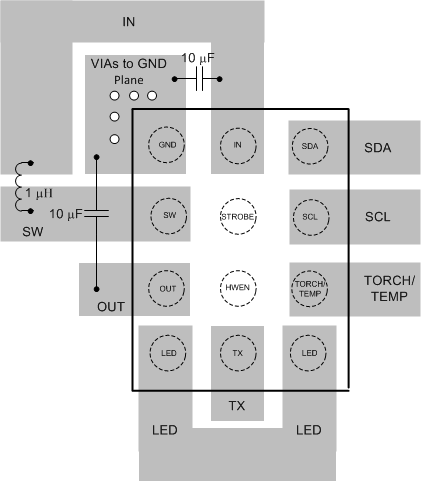 Figure 43. LM3648 Layout Example