SNVS782C October 2010 – August 2015 LM3243
PRODUCTION DATA.
- 1 Features
- 2 Applications
- 3 Description
- 4 Revision History
- 5 Pin Configuration and Functions
- 6 Specifications
- 7 Detailed Description
- 8 Application and Implementation
- 9 Power Supply Recommendations
- 10Layout
- 11Device and Documentation Support
- 12Mechanical, Packaging, and Orderable Information
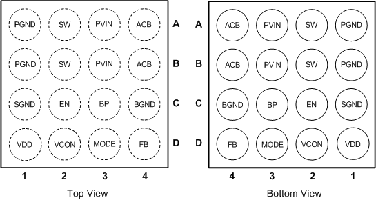
5 Pin Configuration and Functions
TMD Package
16-Pin DSBGA

Pin Functions
| PIN | TYPE | DESCRIPTION | |
|---|---|---|---|
| NO. | NAME | ||
| A1 | PGND | Ground | Power ground to the internal NFET switch. |
| B1 | |||
| C1 | SGND | Ground | Signal analog and control ground (low current). |
| D1 | VDD | Power | Analog supply input. |
| A2 | SW | Analog | Switching node connection to the internal PFET switch and NFET synchronous rectifier. Connect to an inductor with a saturation current rating that exceeds the ILIM,PFET,Steady State current limit specification of the LM3243. |
| B2 | |||
| C2 | EN | Digital/Input | Enable input. Set this digital input HIGH for normal operation. For shutdown, set low. Pin has an 800-kΩ internal pulldown resistor. |
| D2 | VCON | Analog | Voltage control analog input. VOUT = 2.5 × VCON. |
| A3 | PVIN | Power | Power supply voltage input to the internal PFET switch and ACB. |
| B3 | |||
| C3 | BP | Digital | Bypass mode input. Set the pin HIGH for forced Bypass mode operation. Set the pin LOW for automatic analog bypass mode (recommended). |
| D3 | MODE | Digital/Input | PWM/PFM mode selection input. Setting the pin HIGH allows for PFM or PWM, depending on the load current. Setting the pin LOW forces the part to be in PWM only. |
| A4 | ACB | Output | Analog Current Bypass (ACB). Connect to the output at the output filter capacitor. |
| B4 | |||
| C4 | BGND | Ground | ACB ground (high current). |
| D4 | FB | Analog | Feedback analog input. Connect to the output at the output filter capacitor. |