SNVS782C October 2010 – August 2015 LM3243
PRODUCTION DATA.
- 1 Features
- 2 Applications
- 3 Description
- 4 Revision History
- 5 Pin Configuration and Functions
- 6 Specifications
- 7 Detailed Description
- 8 Application and Implementation
- 9 Power Supply Recommendations
- 10Layout
- 11Device and Documentation Support
- 12Mechanical, Packaging, and Orderable Information
8 Application and Implementation
NOTE
Information in the following applications sections is not part of the TI component specification, and TI does not warrant its accuracy or completeness. TI’s customers are responsible for determining suitability of components for their purposes. Customers should validate and test their design implementation to confirm system functionality.
8.1 Application Information
The LM3243 DC-DC converter steps down an input voltage from 2.7 V to 5.5 V to a dynamically adjustable output voltage of 0.4 V to 3.6 V.
8.2 Typical Application
 Figure 17. LM3243 Typical Application
8.2.1 Design Requirements
For typical step-down converter applications, use the parameters listed in Table 2.
Table 2. Design Parameters
| DESIGN PARAMETER | EXAMPLE VALUE |
|---|---|
| Input voltage | 2.7 V to 5.5 V |
| Minimum output voltage | 0.4 V to 3.6 V |
| Output current range | 0 to 2.5 A |
8.2.2 Detailed Design Procedure
8.2.2.1 Inductor Selection
A 1.5 µH inductor is needed for optimum performance and functionality of the LM3243. In the case of 2G transmission current bursts, the effective overall RMS current requirements are reduced. Therefore, please consult with the inductor manufacturers to determine if some of their smaller components will meet your application needs even though the classical inductor specification does not appear to meet the LM3243 RMS current specifications.
LM3243 automatically manages the inductor peak and RMS (or steady current peak) current through the SW pin. The SW pin has two positive current limits. The first is the 1.45 A typical (or 1.65 A maximum.) over-limit current protection. It sets the upper steady-state inductor peak current (as detailed in the Electrical Characteristics Table - ILIM,PFET,SteadyState). It is the dominant factor limiting the inductor's ISAT requirement. The second is a over-limit current protection. It limits the maximum peak inductor current during large signal transients (that is, < 20 µs) to 1.9 A typical (or 2.1 A maximum). A minimum inductance of 0.3 µH should be maintained at the second current limit.
The ACB circuit automatically adjusts its output current to keep the steady-state inductor current below the steady-state peak current limit. Thus, the inductor RMS current will effectively always be less than the ILIM,PFET,SteadyState during the transmit burst. In addition, as in the case with 2G where the output current comes in bursts, the effective overall RMS current would be much lower.
For good efficiency, the inductor’s resistance should be less than 0.2 Ω; low DCR inductors (< 0.2 Ω) are recommended. Table 3 suggests some inductors and suppliers.
Table 3. Suggested Inductors and Their Suppliers
| MODEL | VENDOR | SIZE (mm) | ISAT −30% | DCR |
|---|---|---|---|---|
| DFE201610C-1R5M (1285AS-H-1R5M) |
TOKO | 2 × 1.6 × 1 | 2.2 A | 120 mΩ |
| PSD20161T-1R5MS | CYNTEC | 2 × 1.6 × 1 | 1.6 A | 143 mΩ |
| TFM201610-1R5M | TDK | 2 × 1.6 mm × 1 | 2.2 A | 140 mΩ |
8.2.2.2 Capacitor Selection
The LM3243 is designed to use ceramic capacitors for its input and output filters. Use a 10-µF capacitor for the input and approximately 10-µF total output capacitance. Capacitor types such as X5R, X7R are recommended for both filters. These provide an optimal balance between small size, cost, reliability and performance for cell phones and similar applications. Table 4 lists suggested part numbers and suppliers. DC bias characteristics of the capacitors must be considered while selecting the voltage rating and case size of the capacitor. Smaller case sizes for the output capacitor mitigate piezo-electric vibrations of the capacitor when the output voltage is stepped up and down at fast rates. However, they have a bigger percentage drop in value with DC bias. For even smaller total solution size, 0402 case size capacitors are recommended for filtering. Use of multiple 2.2-µF or 1-µF capacitors can also be considered. For RF Power Amplifier applications, split the output capacitor between DC-DC converter and RF Power Amplifiers: 10 µF (COUT1) + 4.7 µF (COUT2) + 3 × 1 µF (COUT3) is recommended. The optimum capacitance split is application dependent, and for stability the actual total capacitance (taking into account effects of capacitor DC bias, temperature de-rating, aging and other capacitor tolerances) should target 10 µF with 2.5-V DC bias (measured at 0.5 VRMS). Place all the output capacitors very close to the respective device. A high-frequency capacitor (3300 pF) is highly recommended to be placed next to COUT1.
Table 4. Suggested Capacitors And Their Suppliers
| CAPACITANCE | MODEL | SIZE (W × L) (mm) | VENDOR |
|---|---|---|---|
| 10 µF | GRM185R60J106M | 1.6 × 0.8 | Murata |
| 10 µF | CL05A106MQ5NUN | 1 × 0.5 | Samsung |
| 4.7 µF | CL05A475MQ5NRN | 1 × 0.5 | Samsung |
| 1.0 µF | CL03A105MQ3CSN | 0.6 × 0.3 | Samsung |
| 3300 pF | GRM022R60J332K | 0.4 × 0.2 | Murata |
8.2.2.3 Setting The Output Voltage
8.2.2.3.1 DAC Control
An analog voltage to the VCON pin can dynamically program the output voltage from 0.4 V (typical) to 3.6 V (typical) in both PFM and PWM modes of operation, without the need for external resistors. The output voltage is governed by Table 5.
Table 5. Output Voltage Selection
| VCON (V) | VOUT (V) |
|---|---|
| VCON = 0.16V to 1.44V | 2.5 × VCON |
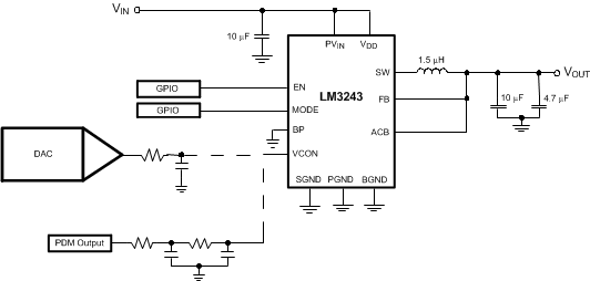 Figure 18. Dynamic Adjustment of Output Voltage With DAC or PDM
8.2.2.3.2 PDM-Based VCON Signal
Figure 18 shows the application circuit that enables the LM3243 to dynamically adjust the output voltage using a GPIO pin from the system controller. Figure 19 shows the waveforms when adjusted dynamically. The PDM signal of the GPIO is filtered using a low-pass filter and fed to the VCON pin. As the bitstream of the PDM signal changes, the voltage on the VCON pin changes. Thus, the GPIO pin can be used to dynamically adjust the output voltage. The double low-pass filter reduces the ripple at VCON to avoid any excessive VCON-induced ripple at the output voltage.
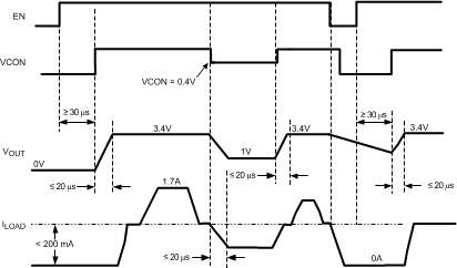 Figure 19. Dynamic Adjustment of Output Voltage With GPIO
8.2.2.3.3 VCON Pin
Figure 20 shows the equivalent CRC circuit for the VCON pin. This circuit is internal to the part and should be taken into consideration when driving this pin.
 Figure 20. VCON Pin Equivalent CRC Circuit
8.2.2.4 EN Input Control
Use the system controller to drive the EN HIGH or LOW with a comparator, Schmitt trigger or logic gate. Set EN = HIGH (> 1.2 V) for normal operation and LOW (< 0.5 V) for shutdown mode to reduce current consumption to 0.02-µA (typical) current.
8.2.2.5 Start-Up
The waveform Figure 21 in shows the start-up condition. First, VIN should take on a value between 2.7 V and 5.5 V. Next, EN should go HIGH (> 1.2 V). Finally, VCON should be set to a value that corresponds to the required output voltage (VOUT = VCON × 2.5). VOUT will reach its steady-state value in less than 50 µs. To optimize the start-up time and behavior of the output voltage, the LM3243 will always start up in PWM mode (even when MODE = HIGH and output load current ≤ 75 mA), then seamlessly transition into PFM mode.
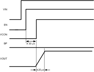 Figure 21. Start-Up Sequence and Conditions
8.2.3 Application Curves
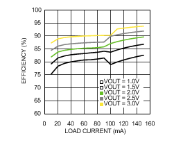
| VIN = 3.8 V |
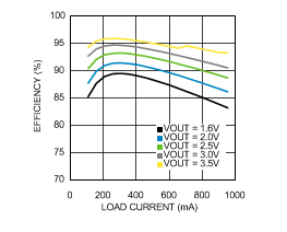
| VIN = 3.8 V | IOUT = 100 mA To 1 A |
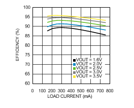
| VIN = 3.8 V | IOUT = 150 mA To 750 mA | |
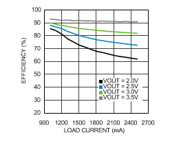
| VIN = 3.8 V | IOUT = 1 A To 2.5 A |