SNVS770I June 1999 – January 2015 LM2941 , LM2941C
PRODUCTION DATA.
- 1 Features
- 2 Applications
- 3 Description
- 4 Revision History
- 5 Pin Configuration and Functions
- 6 Specifications
- 7 Detailed Description
- 8 Application and Implementation
- 9 Power Supply Recommendations
- 10Layout
- 11Device and Documentation Support
- 12Mechanical, Packaging, and Orderable Information
封装选项
请参考 PDF 数据表获取器件具体的封装图。
机械数据 (封装 | 引脚)
- NDH|5
- NGN|8
- KTT|5
- KC|5
散热焊盘机械数据 (封装 | 引脚)
- KTT|5
订购信息
6 Specifications
6.1 Absolute Maximum Ratings(1)(2)
| MIN | MAX | UNIT | ||
|---|---|---|---|---|
| Input voltage (Survival Voltage, ≤ 100 ms) | LM2941T, LM2941S, LM2941LD | 60 | V | |
| LM2941CT, LM2941CS | 45 | V | ||
| Internal power dissipation (3) | Internally Limited | |||
| Maximum junction temperature | 150 | °C | ||
| Soldering remperature(4) | TO-220 (T), Wave, 10 s | 260 | °C | |
| TO-263 (S), 30 s | 235 | °C | ||
| WSON-8 (LD), 30 s | 235 | °C | ||
| Storage temperature, Tstg | −65 | 150 | °C | |
(1) Stresses beyond those listed under Absolute Maximum Ratings may cause permanent damage to the device. These are stress ratings only, which do not imply functional operation of the device at these or any other conditions beyond those indicated under Recommended Operating Conditions. Exposure to absolute-maximum-rated conditions for extended periods may affect device reliability.
(2) If Military/Aerospace specified devices are required, please contact the Texas Instruments Sales Office/Distributors for availability and specifications.
(3) The maximum power dissipation is a function of TJ(max), RθJA, and TA. The maximum allowable power dissipation at any ambient temperature is PD = (TJ(max) − TA)/RθJA. If this dissipation is exceeded, the die temperature will rise above 150°C and the LM2941 will go into thermal shutdown. If the TO-263 package is used, the thermal resistance can be reduced by increasing the PC board copper area thermally connected to the package. The value RθJA for the WSON package is specifically dependent on PCB trace area, trace material, and the number of layers and thermal vias. For improved thermal resistance and power dissipation for the WSON package, refer to Application Note AN-1187 (SNOA401). It is recommended that 6 vias be placed under the center pad to improve thermal performance.
(4) Refer to JEDEC J-STD-020C for surface mount device (SMD) package reflow profiles and conditions. Unless otherwise stated, the temperature and time are for Sn-Pb (STD) only.
6.2 ESD Ratings
| VALUE | UNIT | |||
|---|---|---|---|---|
| V(ESD) | Electrostatic discharge | Human-body model (HBM), per ANSI/ESDA/JEDEC JS-001(1) | ±2000 | V |
(1) JEDEC document JEP155 states that 500-V HBM allows safe manufacturing with a standard ESD control process.
6.3 Recommended Operating Conditions
| MIN | MAX | UNIT | ||
|---|---|---|---|---|
| Temperatures | LM2941T | −40 | 125 | °C |
| LM2941CT | 0 | 125 | ||
| LM2941S | −40 | 125 | ||
| LM2941CS | 0 | 125 | ||
| LM2941LD | −40 | 125 | ||
6.4 Thermal Information
| THERMAL METRIC(1)(3) | LM2941LD | LM2941S, LM2941T | UNIT | ||
|---|---|---|---|---|---|
| WSON (NGN) | TO-263 (KTT) | TO-220 (KC) | |||
| 8 PINS | 5 PINS | 5 PINS | |||
| RθJA | Junction-to-ambient thermal resistance | 40.5 | 41 | 32.1 | °C/W |
| RθJC(top) | Junction-to-case (top) thermal resistance | 26.2 | 43.2 | 25.6 | |
| RθJB | Junction-to-board thermal resistance | 17 | 22.9 | 18.3 | |
| ψJT | Junction-to-top characterization parameter | 0.2 | 11.4 | 8.5 | |
| ψJB | Junction-to-board characterization parameter | 17.2 | 21.9 | 17.7 | |
| RθJC(bot) | Junction-to-case (bottom) thermal resistance | 3.2 | 0.9 | 0.7 | |
(1) For more information about traditional and new thermal metrics, see the IC Package Thermal Metrics application report, SPRA953.
6.5 Electrical Characteristics: LM2941T, LM2941S, LM2941LD
5 V ≤ VOUT ≤ 20 V, VIN = VOUT + 5 V, COUT = 22 μF, unless otherwise specified. MIN (minimum) and MAX (maximum) specifications in apply over the full Operating Temperature Range (unless otherwise specified) and typical values apply at TJ = 25°C.| PARAMETER | TEST CONDITIONS | MIN | TYP | MAX | UNIT |
|---|---|---|---|---|---|
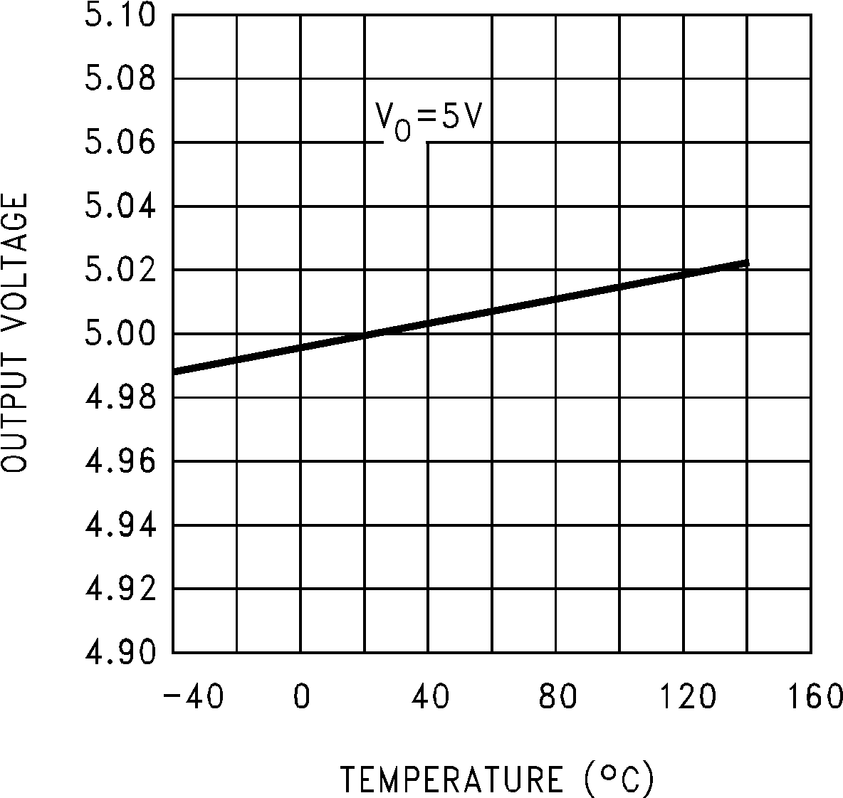
| Reference voltage | 5 mA ≤ IOUT ≤ 1 A(1) | 1.211 | 1.275 | 1.339 | V |
| 5 mA ≤ IOUT ≤ 1 A(1), TJ = 25°C | 1.237 | 1.275 | 1.313 | ||
| Line regulation | VOUT + 2 V ≤ VIN ≤ 26 V, IOUT = 5 mA | 4 | 10 | mV/V | |
| Load regulation | 50 mA ≤ IOUT ≤ 1 A | 7 | 10 | mV/V | |
| Output impedance | 100 mADC and 20 mArms, ƒOUT = 120 Hz | 7 | mΩ/V | ||
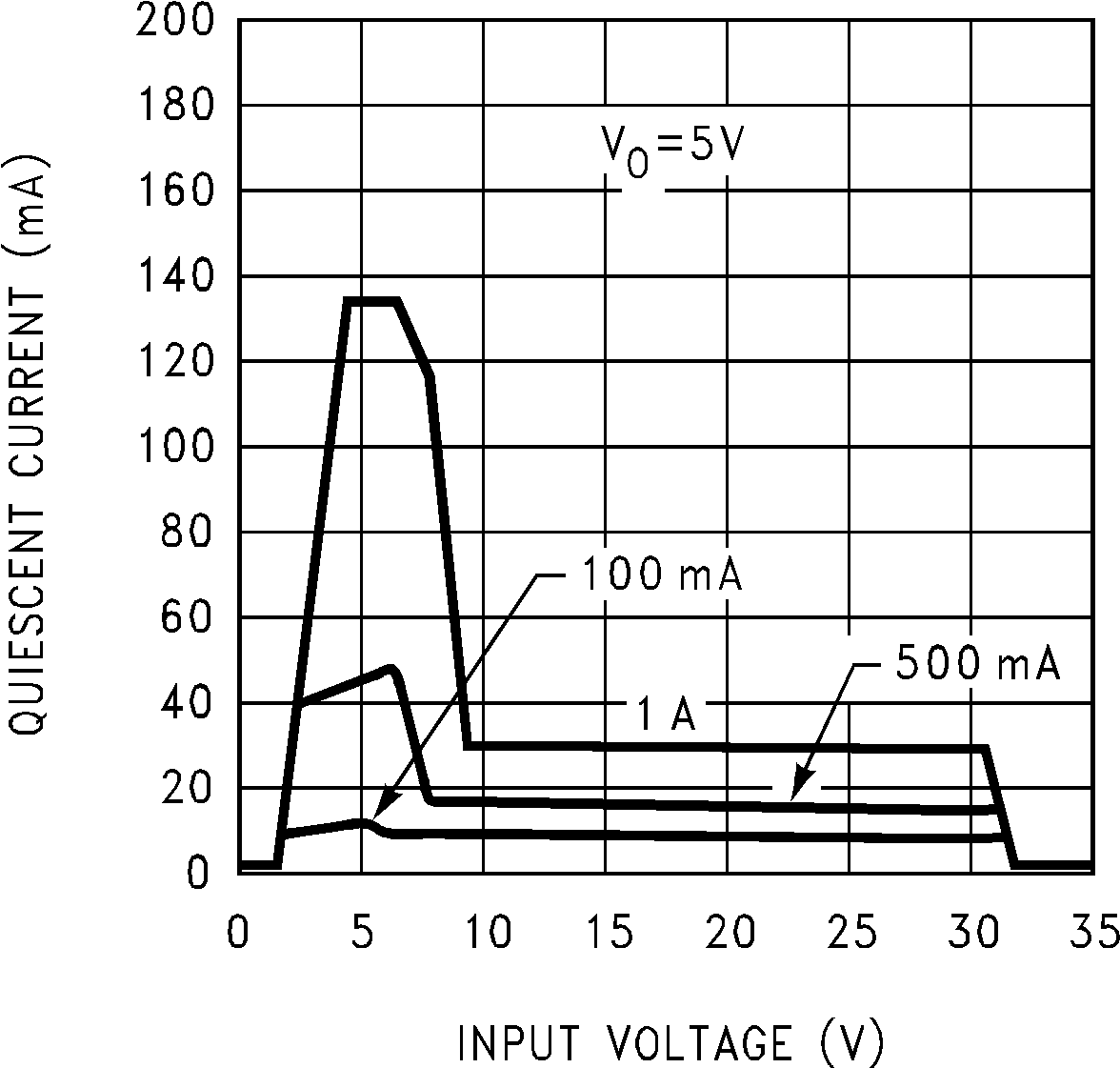
| Quiescent current | VOUT + 2 V ≤ VIN < 26 V, IOUT = 5 mA | 10 | 20 | mA | |
| VOUT + 2 V ≤ VIN < 26 V, IOUT = 5 mA, TJ = 25°C | 10 | 15 | |||
| VIN = VOUT + 5 V, IOUT = 1 A | 30 | 60 | mA | ||
| VIN = VOUT + 5 V, IOUT = 1 A, TJ = 25°C | 30 | 45 | |||
| RMS output noise, % of VOUT | 10 Hz to 100 kHz, IOUT = 5 mA | 0.003% | |||
| Ripple rejection | ƒOUT = 120 Hz, 1 Vrms, IL = 100 mA | 0.005 | 0.04 | %/V | |
| ƒOUT = 120 Hz, 1 Vrms, IL = 100 mA, TJ = 25°C | 0.005 | 0.02 | |||
| Long-term stability | 0.4 | %/1000 Hr | |||
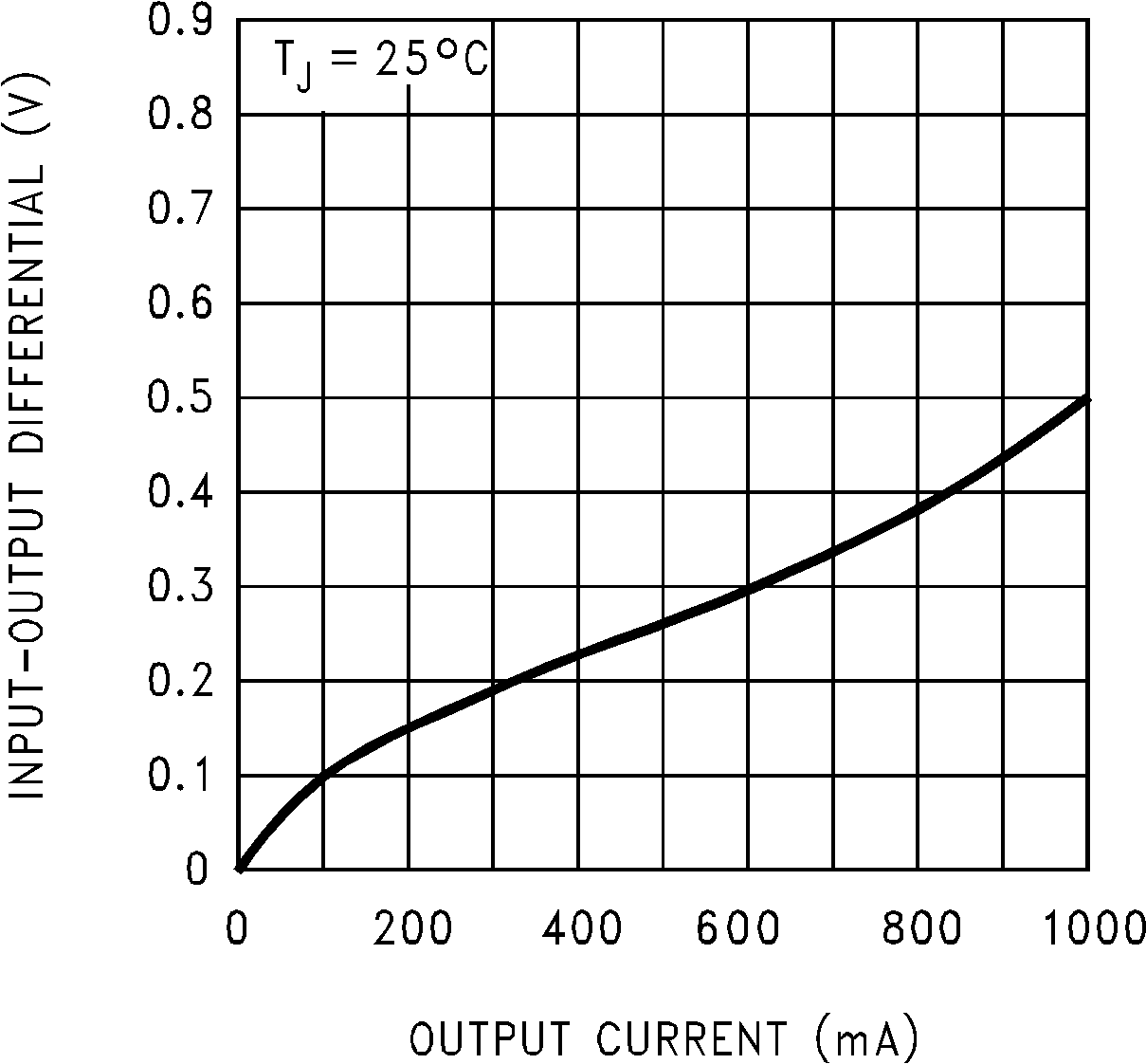
| Dropout voltage | IOUT = 1 A | 0.5 | 1 | V | |
| IOUT = 1 A, TJ = 25°C | 0.5 | 0.8 | |||
| IOUT = 100 mA | 110 | 200 | mV | ||
| Short-circuit current | VIN max = 26 V(2) | 1.6 | 1.9 | A | |
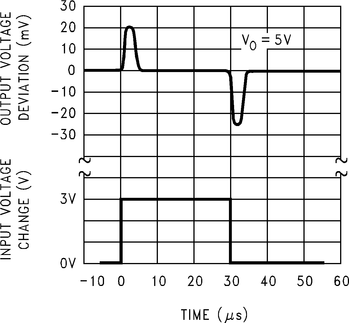
| Maximum line transient | VOUT max 1 V above nominal VOUT
ROUT = 100 Ω, t ≤ 100 ms |
60 | 75 | V | |
| Maximum operational input voltage | 26 | 31 | VDC | ||
| Reverse polarity DC input voltage |
ROUT = 100 Ω, VOUT ≥ −0.6 V | −15 | −30 | V | |
| Reverse polarity transient input voltage |
t ≤ 100 ms, ROUT = 100 Ω | −50 | −75 | ||
| ON/OFF threshold voltage ON |
IOUT ≤ 1 A | 1.30 | 0.80 | V | |
| ON/OFF threshold voltage OFF |
IOUT ≤ 1 A | 2 | 1.3 | ||
| ON/OFF threshold current |
VON/OFF = 2 V, IOUT ≤ 1 A | 50 | 300 | μA | |
| VON/OFF = 2 V, IOUT ≤ 1 A, TJ = 25°C | 50 | 100 |
(1) The output voltage range is 5 V to 20 V and is determined by the two external resistors, R1 and R2. See Figure 18.
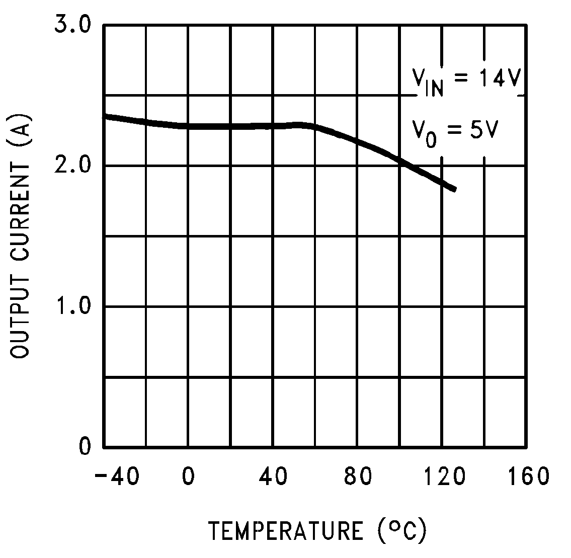
(2) Output current capability will decrease with increasing temperature, but will not go below 1 A at the maximum specified temperatures.
6.6 Electrical Characteristics: LM2941CT, LM2941CS
5 V ≤ VOUT ≤ 20 V, VIN = VOUT + 5 V, COUT = 22 μF, unless otherwise specified. MIN (minimum) and MAX (maximum) specifications in apply over the full Operating Temperature Range (unless otherwise specified) and typical values apply at TJ = 25°C.| PARAMETER | TEST CONDITIONS | MIN | TYP | MAX | UNIT |
|---|---|---|---|---|---|
| Reference voltage | 5 mA ≤ IOUT ≤ 1 A(1) | 1.211 | 1.275 | 1.339 | V |
| 5 mA ≤ IOUT ≤ 1 A(1), TJ = 25°C | 1.237 | 1.275 | 1.313 | ||
| Line regulation | VOUT + 2 V ≤ VIN ≤ 26 V, IOUT = 5 mA, TJ = 25°C | 4 | 10 | mV/V | |
| Load regulation | 50 mA ≤ IOUT ≤ 1 A, TJ = 25°C | 7 | 10 | mV/V | |
| Output impedance | 100 mADC and 20 mArms, ƒOUT = 120 Hz | 7 | mΩ/V | ||
| Quiescent current | VOUT + 2 V ≤ VIN < 26 V, IOUT = 5 mA, TJ = 25°C | 10 | 15 | mA | |
| VIN = VOUT + 5 V, IOUT = 1 A | 30 | 60 | mA | ||
| VIN = VOUT + 5 V, IOUT = 1 A, TJ = 25°C | 30 | 45 | |||
| RMS output noise, % of VOUT | 10 Hz to 100 kHz IOUT = 5 mA |
0.003% | |||
| Ripple rejection | ƒOUT = 120Hz, 1 Vrms, IL = 100 mA, TJ = 25°C | 0.005 | 0.02 | %/V | |
| Long-term stability | 0.4 | %/1000 Hr | |||
| Dropout voltage | IOUT = 1A | 0.5 | 1 | V | |
| IOUT = 1A, TJ = 25°C | 0.5 | 0.8 | |||
| IOUT = 100 mA | 110 | 200 | mV | ||
| Short-circuit current | VIN max = 26 V(2), TJ = 25°C | 1.6 | 1.9 | A | |
| Maximum line transient | VOUT max 1 V above nominal VOUT, ROUT = 100 Ω, t ≤ 100 ms, , TJ = 25°C | 45 | 55 | V | |
| Maximum operational input voltage | TJ = 25°C | 26 | 31 | VDC | |
| Reverse polarity DC input voltage |
ROUT = 100 Ω, VOUT ≥ −0.6 V, TJ = 25°C | −15 | −30 | V | |
| Reverse polarity transient input voltage |
t ≤ 100 ms, ROUT = 100 Ω, TJ = 25°C | −45 | −55 | ||
| ON/OFF threshold voltage ON |
IOUT ≤ 1 A, TJ = 25°C | 1.3 | 0.8 | V | |
| ON/OFF threshold voltage OFF |
IOUT ≤ 1 A, TJ = 25°C | 2 | 1.3 | ||
| ON/OFF threshold current |
VON/OFF = 2 V, IOUT ≤ 1 A, TJ = 25°C | 50 | 100 | μA |
(1) The output voltage range is 5 V to 20 V and is determined by the two external resistors, R1 and R2. See Typical Application.
(2) Output current capability will decrease with increasing temperature, but will not go below 1 A at the maximum specified temperatures.
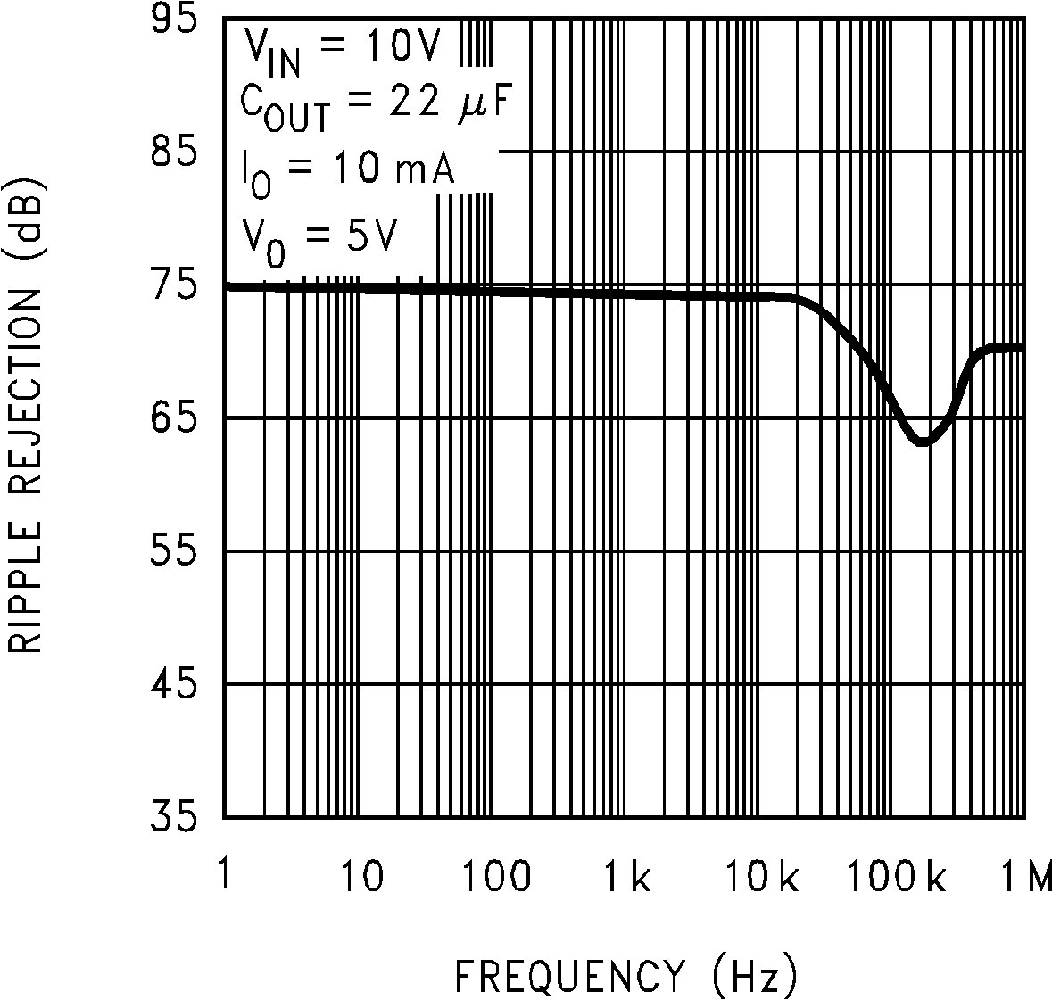
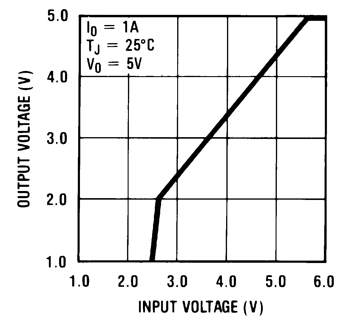
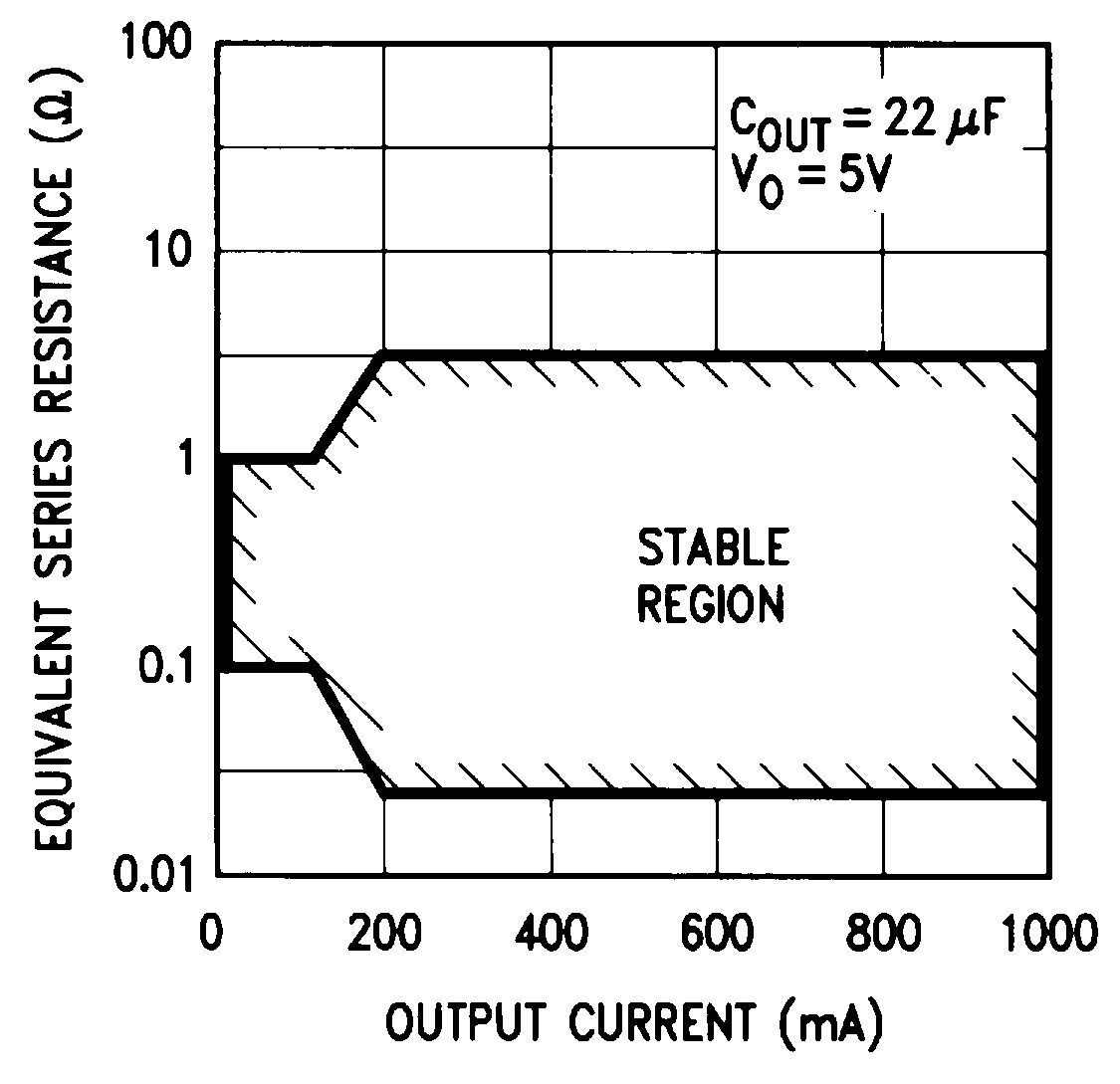
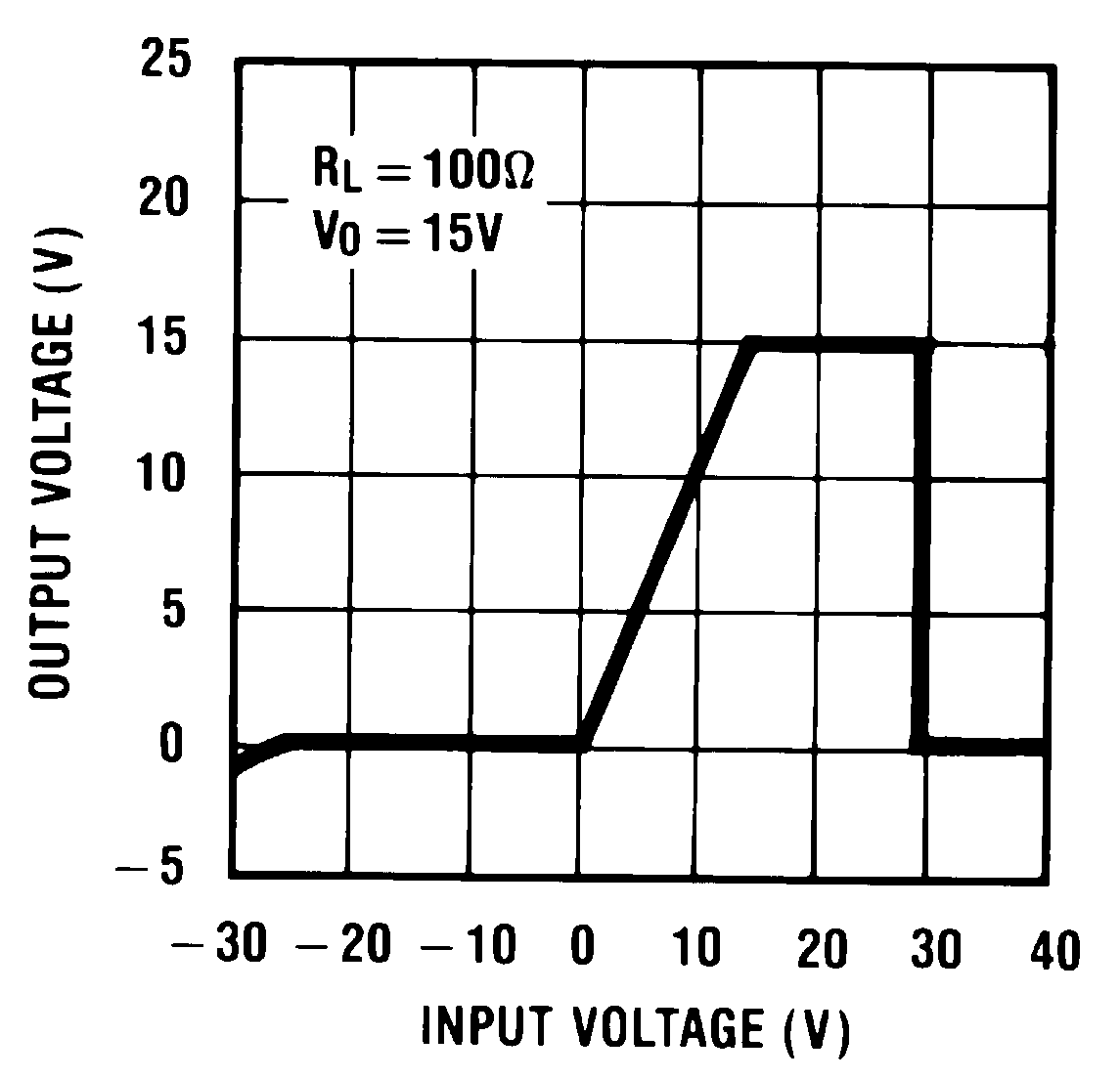
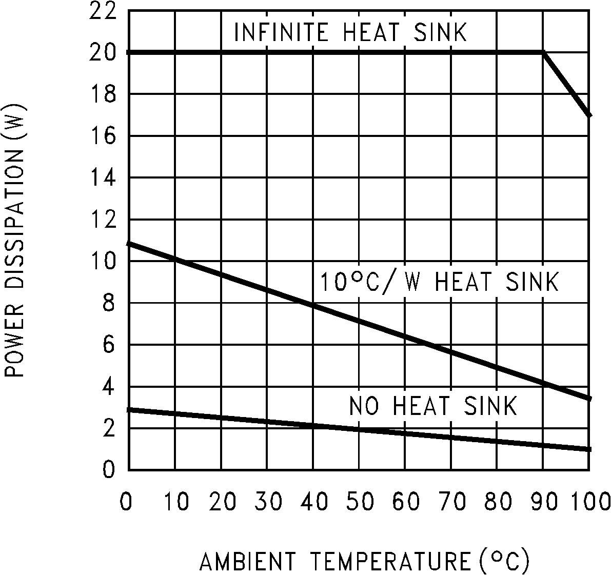
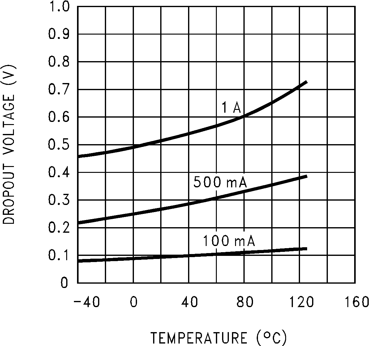
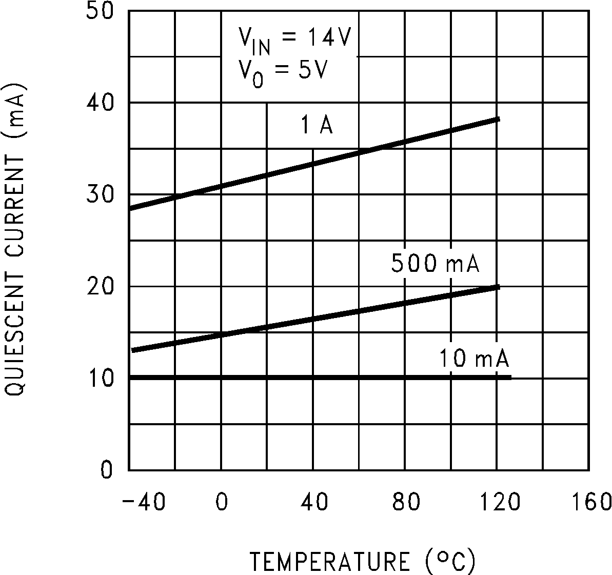
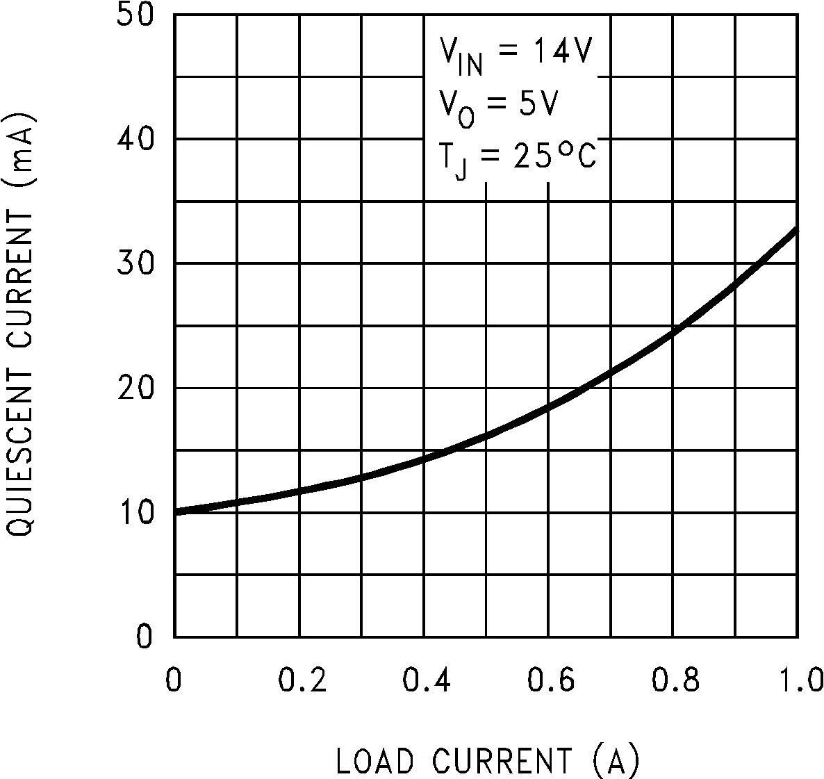
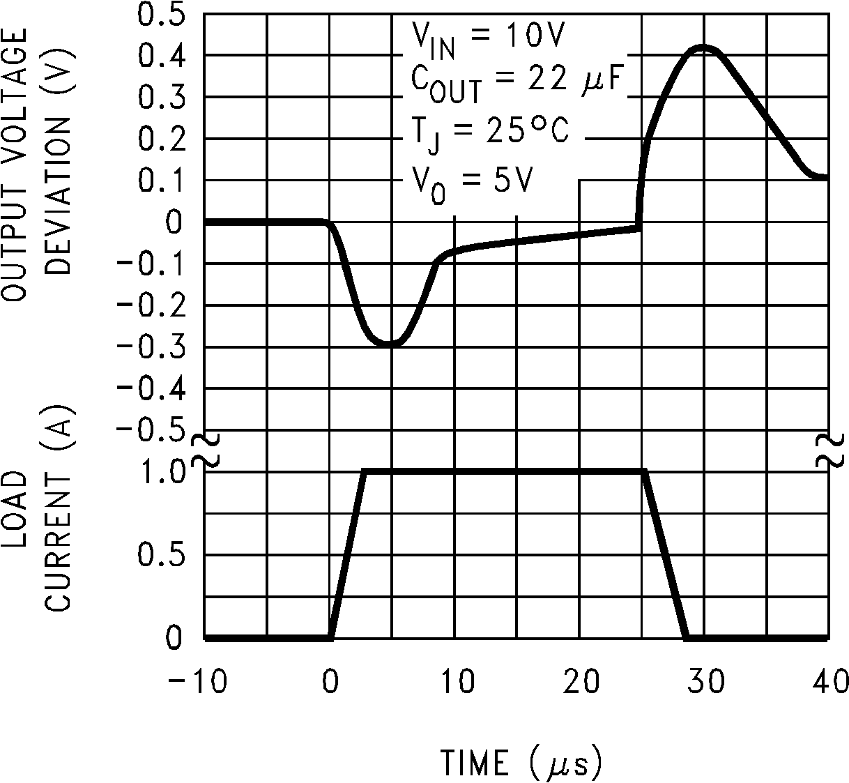
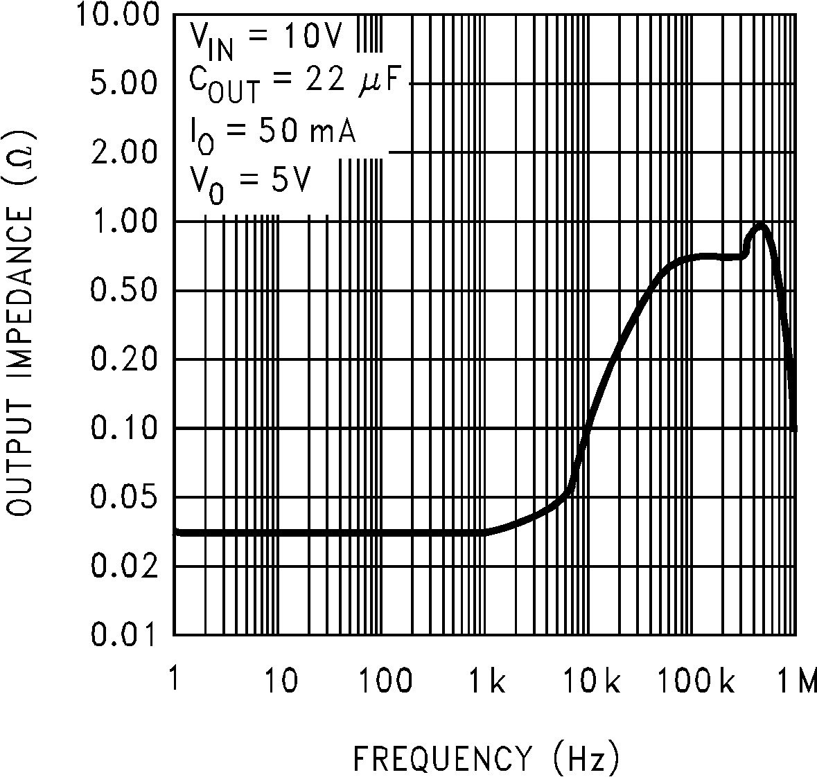
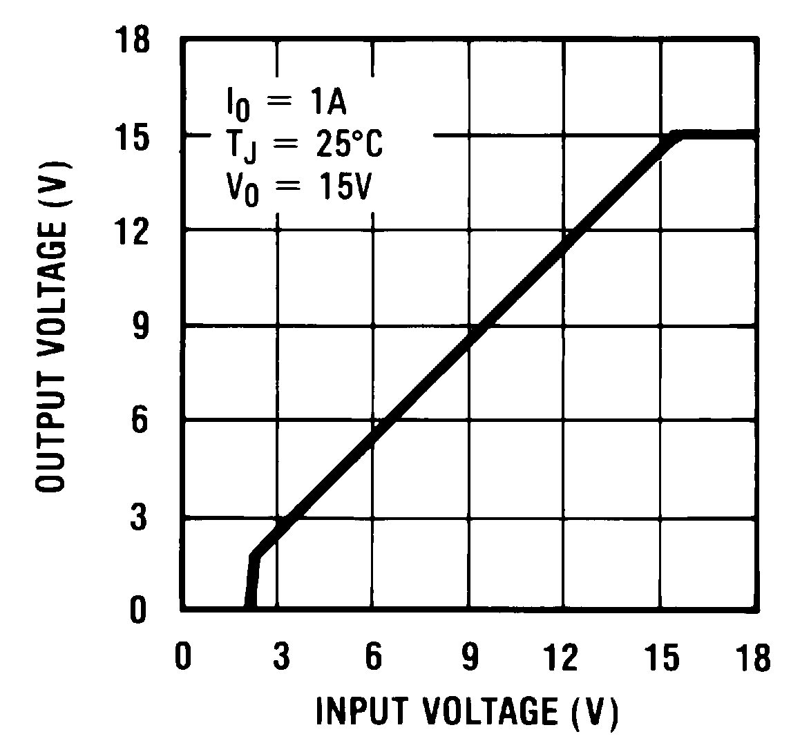
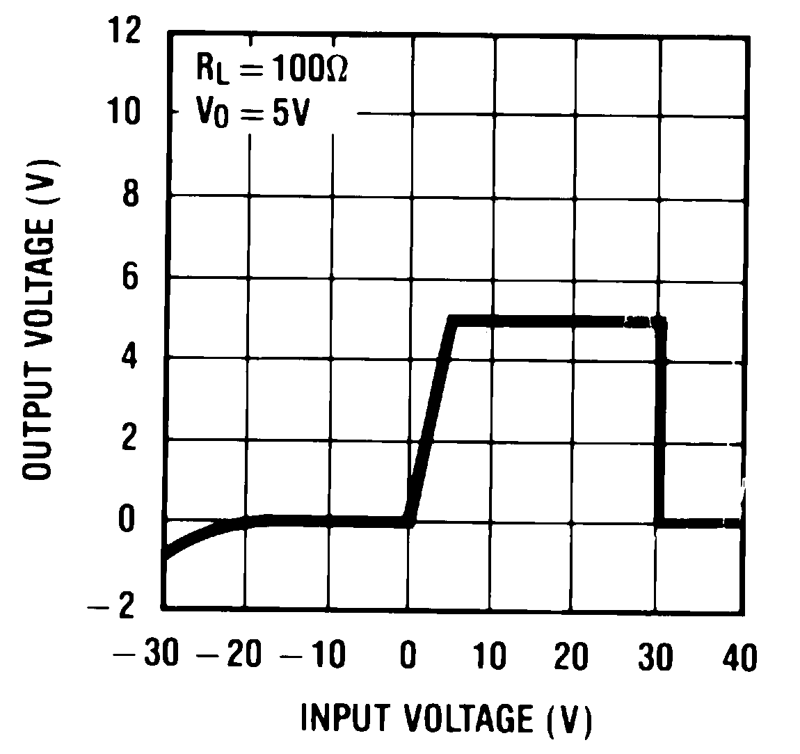
6.7 Typical Characteristics