SNVS770I June 1999 – January 2015 LM2941 , LM2941C
PRODUCTION DATA.
- 1 Features
- 2 Applications
- 3 Description
- 4 Revision History
- 5 Pin Configuration and Functions
- 6 Specifications
- 7 Detailed Description
- 8 Application and Implementation
- 9 Power Supply Recommendations
- 10Layout
- 11Device and Documentation Support
- 12Mechanical, Packaging, and Orderable Information
封装选项
请参考 PDF 数据表获取器件具体的封装图。
机械数据 (封装 | 引脚)
- NDH|5
- NGN|8
- KTT|5
- KC|5
散热焊盘机械数据 (封装 | 引脚)
- KTT|5
订购信息
10 Layout
10.1 Layout Guidelines
The dynamic performance of the LM2941 is dependent on the layout of the PCB. PCB layout practices that are adequate for typical LDOs may degrade the PSRR, noise, or transient performance of the LM2941. Best performance is achieved by placing CIN and COUT on the same side of the PCB as the LM2941, and as close as is practical to the package. The ground connections for CIN and COUT should be back to the LM2941 ground pin using as wide and short of a copper trace as is practical.
10.2 Layout Example
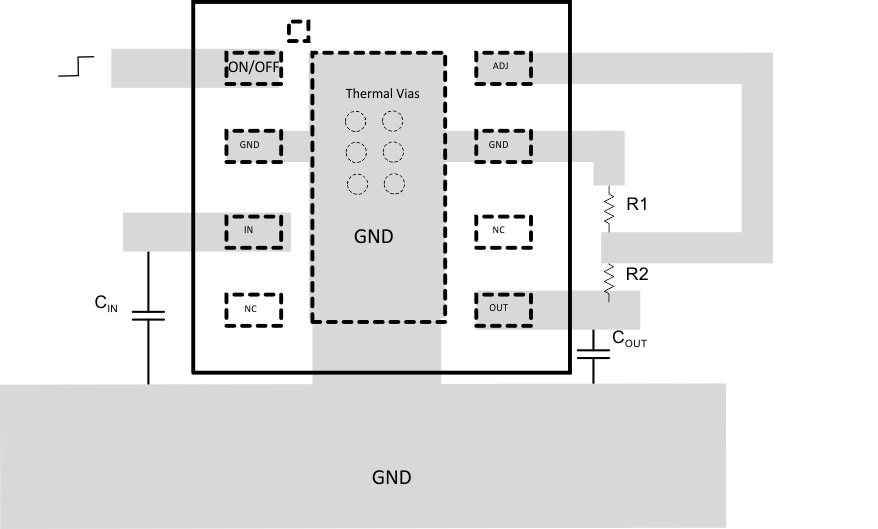 Figure 21. LM2941 WSON Package Typical Layout
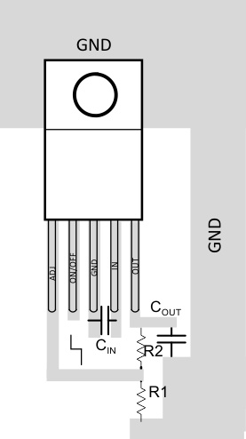 Figure 22. LM2941 TO-220 Package Typical Layout
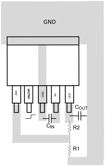 Figure 23. LM2941 TO-263 Package Typical Layout
10.3 Power Dissipation
Consideration should be given to the maximum power dissipation (PD(MAX)) which is limited by the maximum operating junction temperature (TJ(MAX)) of 125°C, the maximum operating ambient temperature (TA(MAX)) of the application, and the thermal resistance (RθJA) of the package. Under all possible conditions, the junction temperature (TJ) must be within the range specified in the Operating Ratings. The total power dissipation of the device is given by:
where IGND is the operating ground pin current of the device (specified under Electrical Characteristics: LM2941T, LM2941S, LM2941LD and Electrical Characteristics: LM2941CT, LM2941CS).
The maximum allowable junction temperature rise (ΔTJ) depends on the maximum expected ambient temperature (TA(MAX)) of the application, and the maximum allowable junction temperature (TJ(MAX)):
The maximum allowable value for junction to ambient Thermal Resistance, RθJA, required to keep the junction temperature, TJ, from exceeding maximum allowed can be calculated using the formula:
The maximum allowable power dissipation, PD(MAX), required allowed for a specific ambient temperature can be calculated using the formula:
Additional information for thermal performance of surface mount packages can be found in AN-1520: A Guide to Board Layout for Best Thermal Resistance for Exposed Packages (SNVA183), AN-1187: Leadless Leadframe Package (LLP) (SNOA401), and AN-2020: Thermal Design By Insight, Not Hindsight (SNVA419).
10.4 Thermal Considerations
10.4.1 TO-263 Mounting
The thermal dissipation of the TO-263 package is directly related to the printed circuit board construction and the amount of additional copper area connected to the TAB.
The TAB on the bottom of the TO-263 package is connected to the die substrate via a conductive die attach adhesive, and to device pin 3. As such, it is strongly recommend that the TAB area be connected to copper area directly under the TAB that is extended into the ground plane via multiple thermal vias. Alternately, but not recommended, the TAB may be left floating (i.e. no direct electrical connection). The TAB must not be connected to any potential other than ground.
10.4.2 WSON Mounting
The NGN (Pullback) 8-Lead WSON package requires specific mounting techniques which are detailed in Application Note 1187: Leadless Leadframe Package (LLP) (SNOA401). Referring to the section PCB Design Recommendations in AN-1187, it should be noted that the pad style which should be used with the WSON package is the NSMD (non-solder mask defined) type.
The thermal dissipation of the WSON package is directly related to the printed circuit board construction and the amount of additional copper area connected to the DAP.
The DAP (exposed pad) on the bottom of the WSON package is connected to the die substrate via a conductive die attach adhesive, and to device pin 2 and pin 7. As such, it is strongly recommend that the DAP area be connected copper area directly under the DAP that is extended into the ground plane via multiple thermal vias. Alternately, but not recommended, the DAP area may be left floating (i.e. no direct electrical connection). The DAP area must not be connected to any potential other than ground.