SNVS454E August 2006 – December 2014 LM2830 , LM2830-Q1
PRODUCTION DATA.
- 1 Features
- 2 Applications
- 3 Description
- 4 Revision History
- 5 Pin Configuration and Functions
- 6 Specifications
- 7 Detailed Description
-
8 Application and Implementation
- 8.1 Application Information
- 8.2
Typical Applications
- 8.2.1 LM2830X Design Vo = 1.2 V at 1.0A
- 8.2.2 LM2830X Design Vo = 0.6 V at 1.0-A
- 8.2.3 LM2830X Design Vo = 3.3 V at 1.0-A
- 8.2.4 LM2830Z Design Vo = 3.3 V at 1.0-A
- 8.2.5 LM2830Z Design Vo = 1.2 V at 1.0-A
- 8.2.6 LM2830X Dual Converters With Delayed Enabled Design
- 8.2.7 LM2830X Buck Converter and Voltage Double Circuit With LDO Follower
- 9 Power Supply Recommendations
- 10Layout
- 11Device and Documentation Support
- 12Mechanical, Packaging, and Orderable Information
6 Specifications
6.1 Absolute Maximum Ratings(1)(2)
| MIN | MAX | UNIT | ||
|---|---|---|---|---|
| VIN | –0.5 | 7 | V | |
| FB Voltage | –0.5 | 3 | V | |
| EN Voltage | –0.5 | 7 | V | |
| SW Voltage | –0.5 | 7 | V | |
| Junction Temperature(1) | 150 | °C | ||
| Tstg | Storage temperature | –65 | 150 | °C |
(1) Stresses beyond those listed under Absolute Maximum Ratings may cause permanent damage to the device. These are stress ratings only, which do not imply functional operation of the device at these or any other conditions beyond those indicated under Recommended Operating Conditions. Exposure to absolute-maximum-rated conditions for extended periods may affect device reliability.
6.2 ESD Ratings: LM2830
| VALUE | UNIT | ||||
|---|---|---|---|---|---|
| V(ESD) | Electrostatic discharge | Human body model (HBM), per ANSI/ESDA/JEDEC JS-001, all pins(1) | ±2000 | V | |
| Charged device model (CDM), per JEDEC specification JESD22-C101, all pins(2) | ±1000 | ||||
(1) JEDEC document JEP155 states that 500-V HBM allows safe manufacturing with a standard ESD control process.
(2) JEDEC document JEP157 states that 250-V CDM allows safe manufacturing with a standard ESD control process.
6.3 ESD Ratings: LM2830-Q1
| VALUE | UNIT | |||||
|---|---|---|---|---|---|---|
| V(ESD) | Electrostatic discharge | Human body model (HBM), per AEC Q100-002(1) | ±2000 | V | ||
| Charged device model (CDM), per AEC Q100-011 | WSON corner pins (1, 3, 4, and 6) | ±1000 | ||||
| SOT-23 corner pins (1, 3, 4, and 5) | ±1000 | |||||
| Other pins | ±1000 | |||||
(1) AEC Q100-002 indicates HBM stressing is done in accordance with the ANSI/ESDA/JEDEC JS-001 specification.
6.4 Recommended Operating Conditions
| MIN | NOM | MAX | UNIT | |
|---|---|---|---|---|
| VIN | 3 | 5.5 | V | |
| Junction Temperature | –40 | 125 | °C |
6.5 Thermal Information
| THERMAL METRIC(1) | LM2830, LM2830-Q1 | LM2830 | UNIT | |
|---|---|---|---|---|
| DBV | NGG | |||
| 5 PINS | 6 PINS | |||
| RθJA | Junction-to-ambient thermal resistance | 165.2 | 53.9 | °C/W |
| RθJC(top) | Junction-to-case (top) thermal resistance | 69.9 | 51.2 | |
| RθJB | Junction-to-board thermal resistance | 27.3 | 28.2 | |
| ψJT | Junction-to-top characterization parameter | 1.8 | 0.6 | |
| ψJB | Junction-to-board characterization parameter | 26.8 | 28.3 | |
| RθJC(bot) | Junction-to-case (bottom) thermal resistance | N/A | 8.1 | |
(1) For more information about traditional and new thermal metrics, see the IC Package Thermal Metrics application report, SPRA953.
6.6 Electrical Characteristics
VIN = 5 V unless otherwise indicated. Typical values correspond to TJ = 25°C. Minimum and maximum limits apply over –40°C to 125°C junction temperature range unless otherwise stated.| PARAMETER | TEST CONDITIONS | MIN | TYP | MAX | UNIT | |
|---|---|---|---|---|---|---|
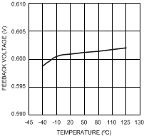
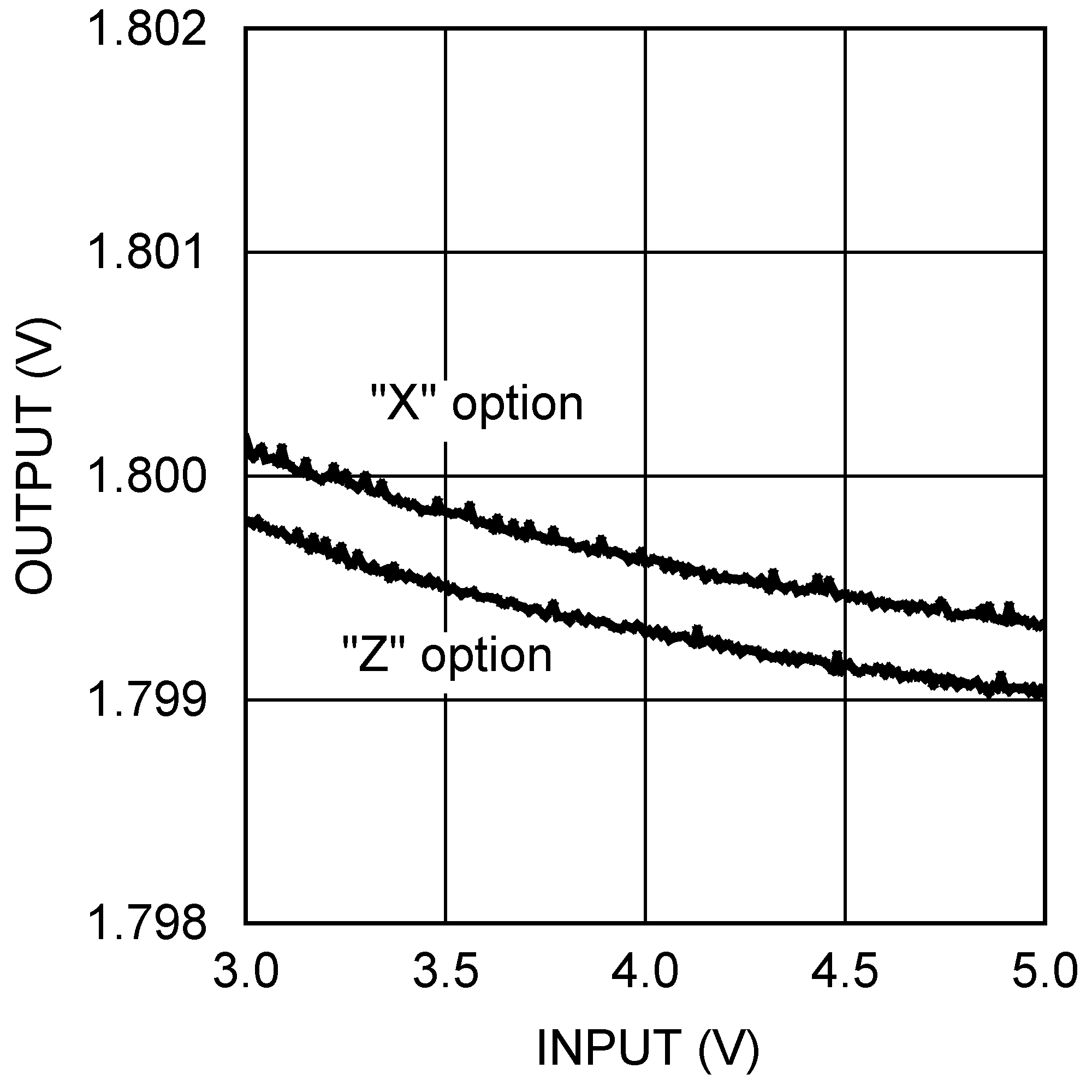
| VFB | Feedback Voltage | WSON and SOT-23 Package | 0.588 | 0.600 | 0.612 | V |
| ΔVFB/VIN | Feedback Voltage Line Regulation | VIN = 3 V to 5 V | 0.02 | %/V | ||
| IB | Feedback Input Bias Current | 0.1 | 100 | nA | ||
| UVLO | Undervoltage Lockout | VIN Rising | 2.73 | 2.90 | V | |
| VIN Falling | 1.85 | 2.3 | ||||
| UVLO Hysteresis | 0.43 | |||||
| FSW | Switching Frequency | LM2830-X | 1.2 | 1.6 | 1.95 | MHz |
| LM2830-Z | 2.25 | 3.0 | 3.75 | |||
| DMAX | Maximum Duty Cycle | LM2830-X | 86% | 94% | ||
| LM2830-Z | 82% | 90% | ||||
| DMIN | Minimum Duty Cycle | LM2830-X | 5% | |||
| LM2830-Z | 7% | |||||
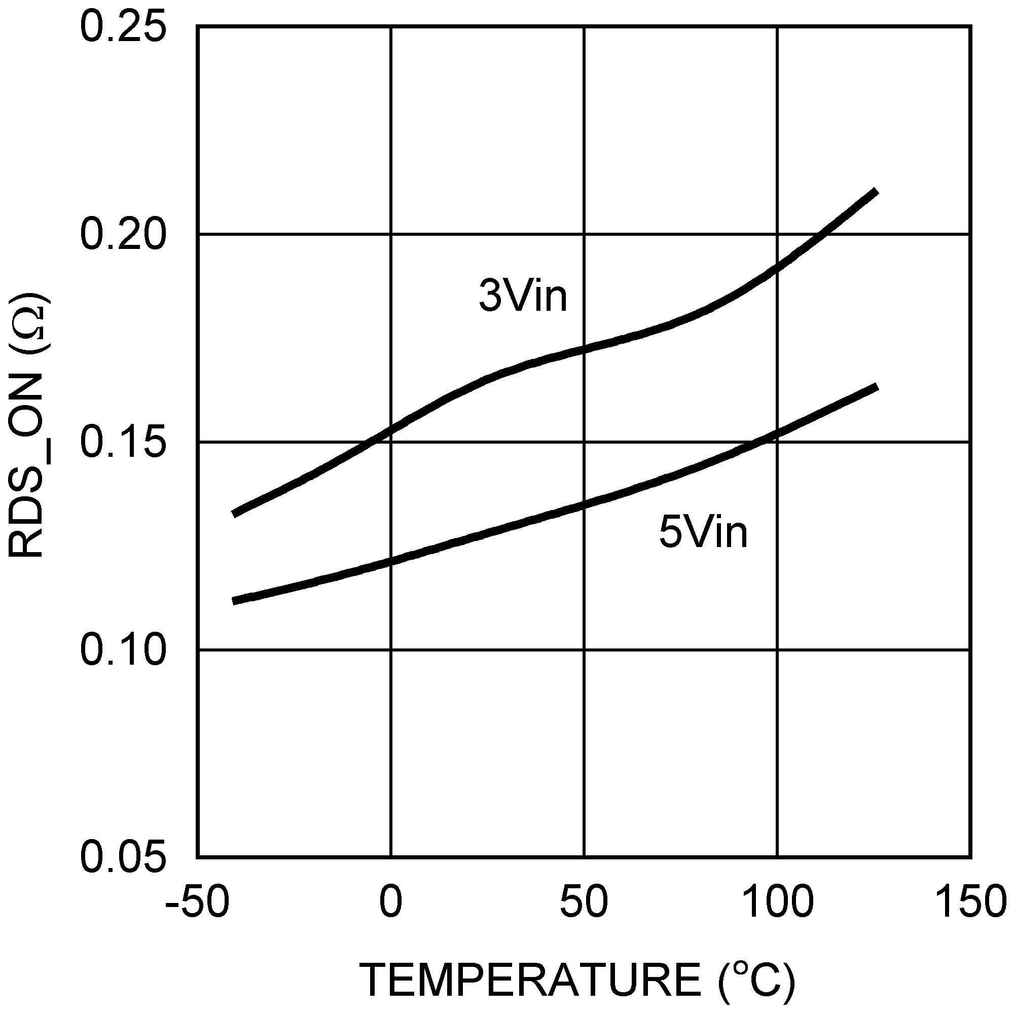
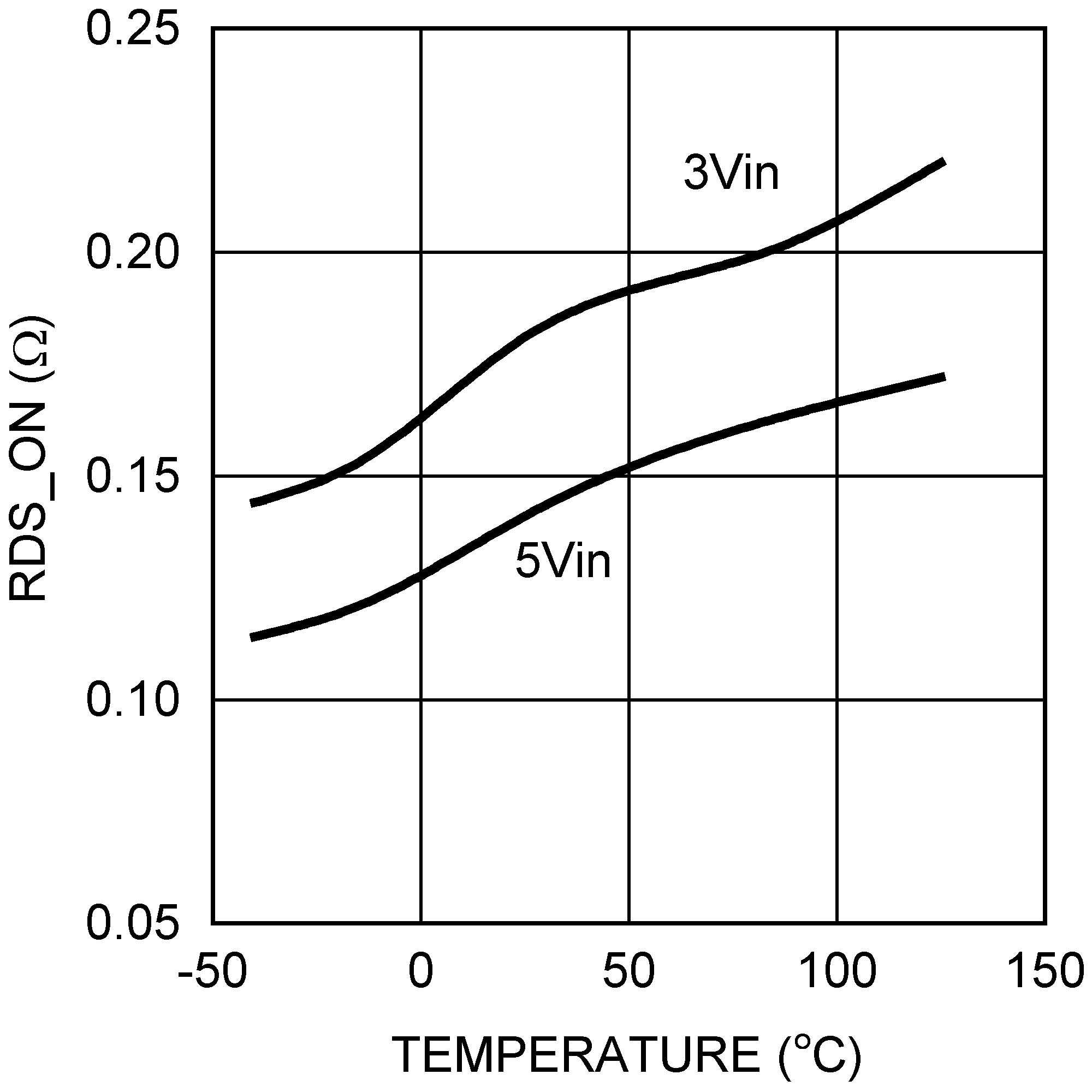
| RDS(ON) | Switch On Resistance | WSON Package | 150 | mΩ | ||
| SOT-23 Package | 130 | 195 | ||||
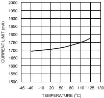
| ICL | Switch Current Limit | VIN = 3.3 V | 1.2 | 1.75 | A | |
| VEN_TH | Shutdown Threshold Voltage | 0.4 | V | |||
| Enable Threshold Voltage | 1.8 | |||||
| ISW | Switch Leakage | 100 | nA | |||
| IEN | Enable Pin Current | Sink/Source | 100 | nA | ||
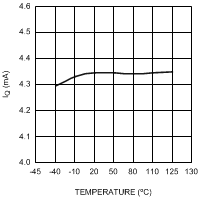
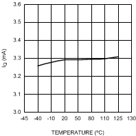
| IQ | Quiescent Current (switching) | LM2830X VFB = 0.55 | 3.3 | 5 | mA | |
| LM2830Z VFB = 0.55 | 4.3 | 6.5 | mA | |||
| Quiescent Current (shutdown) | All Options VEN = 0 V | 30 | nA | |||
| TSD | Thermal Shutdown Temperature | 165 | °C | |||
(1) Thermal shutdown will occur if the junction temperature exceeds the maximum junction temperature of the device.
(2) If Military/Aerospace specified devices are required, please contact the Texas Instruments Sales Office/ Distributors for availability and specifications.
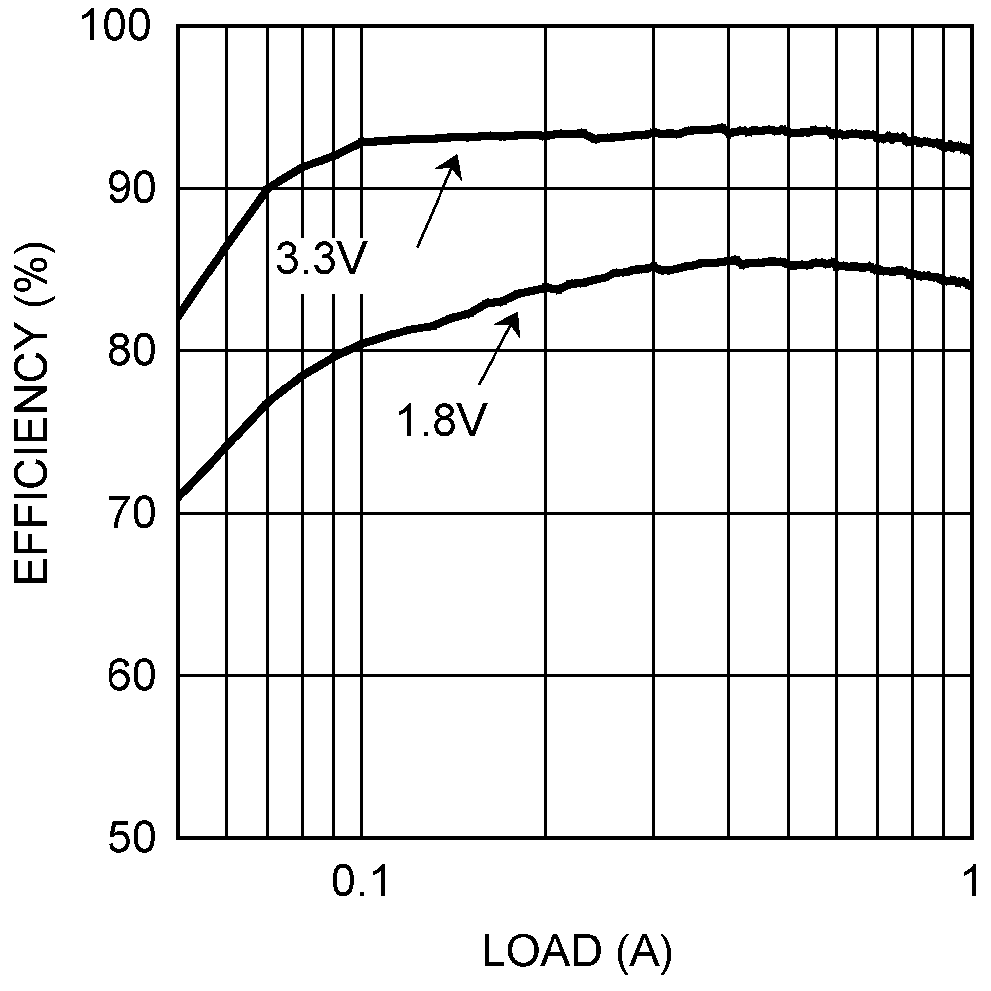
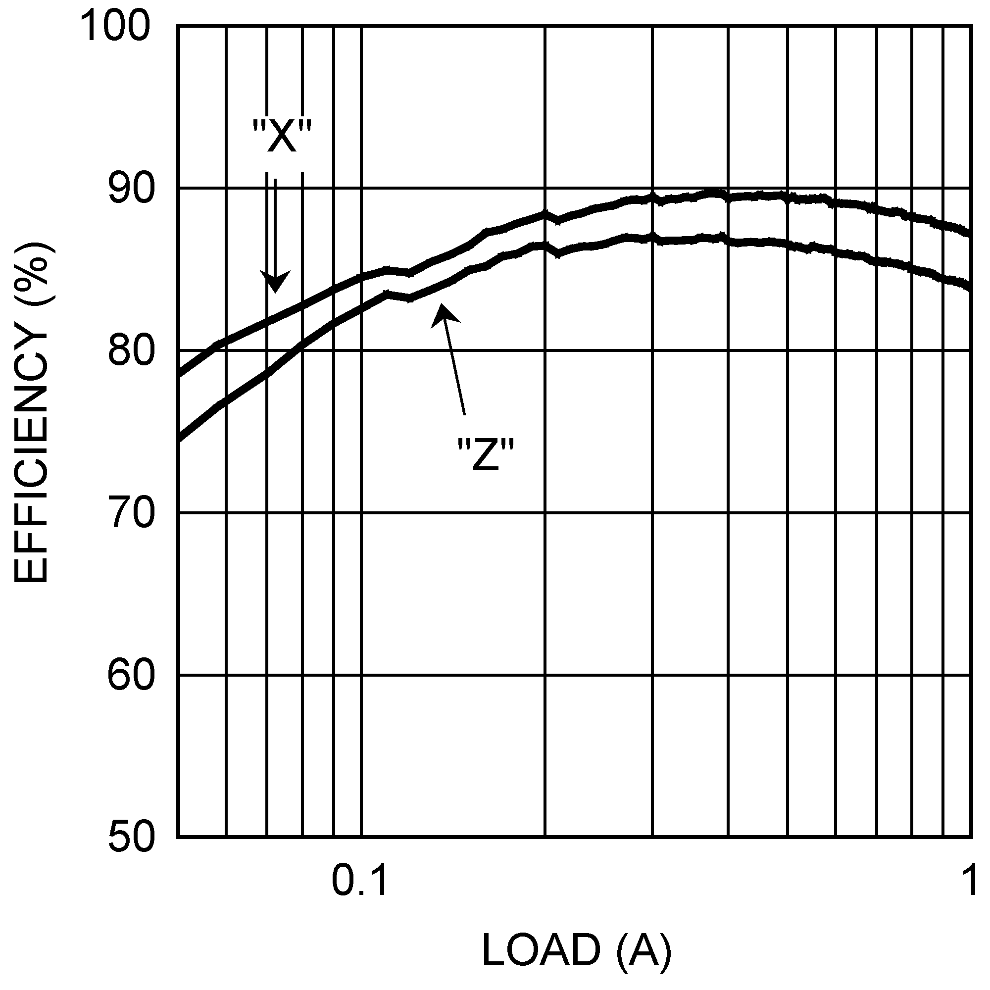
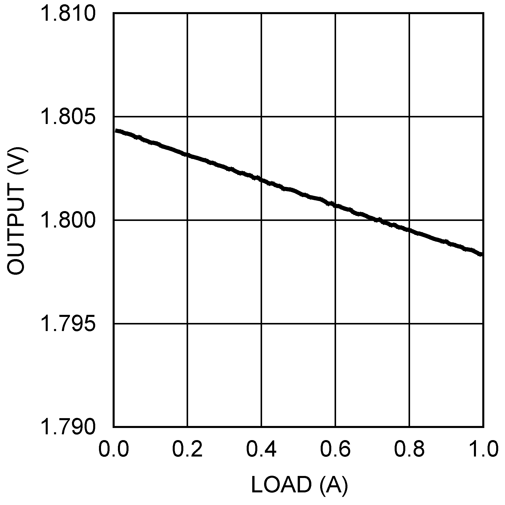
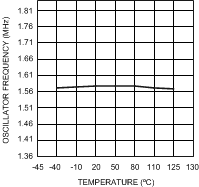
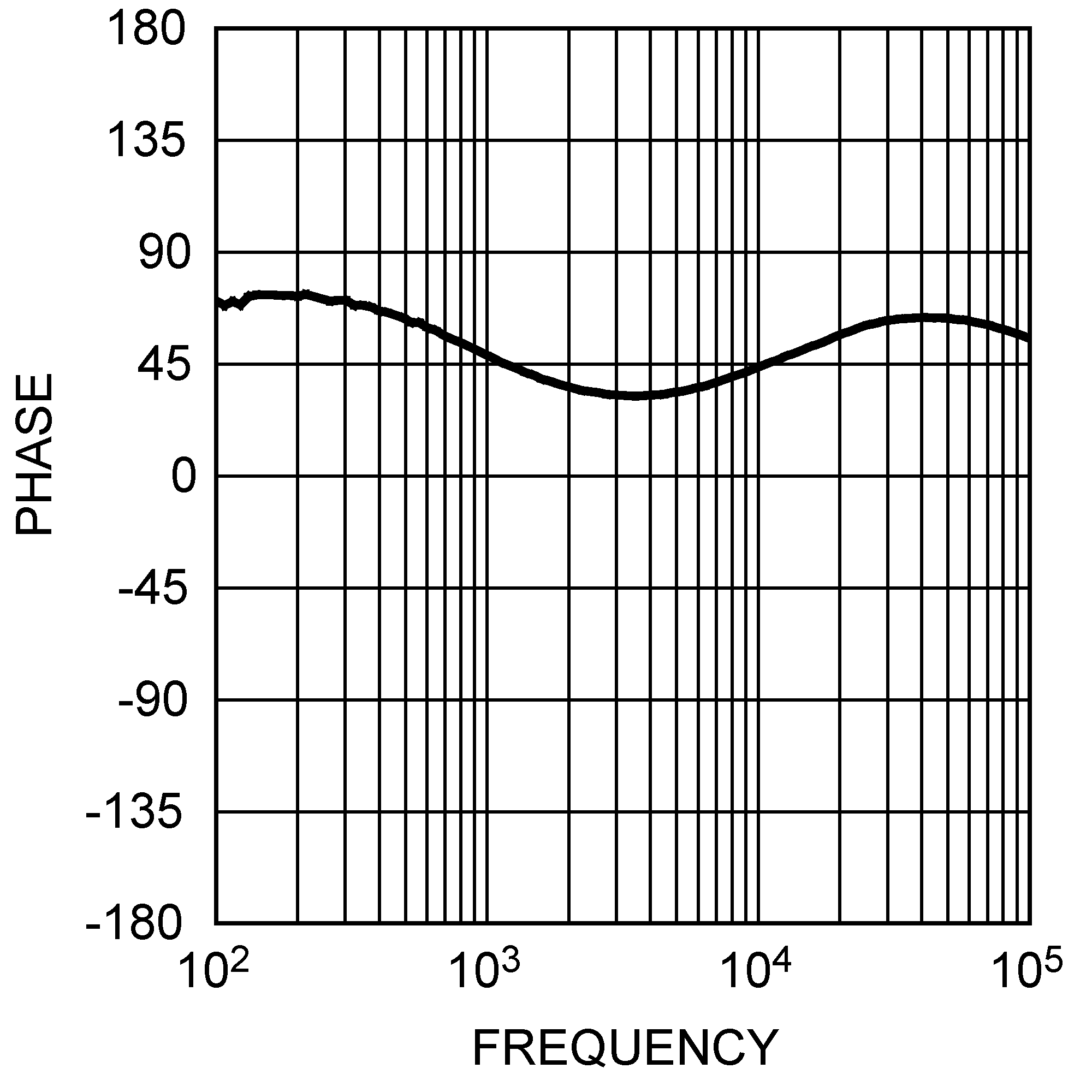
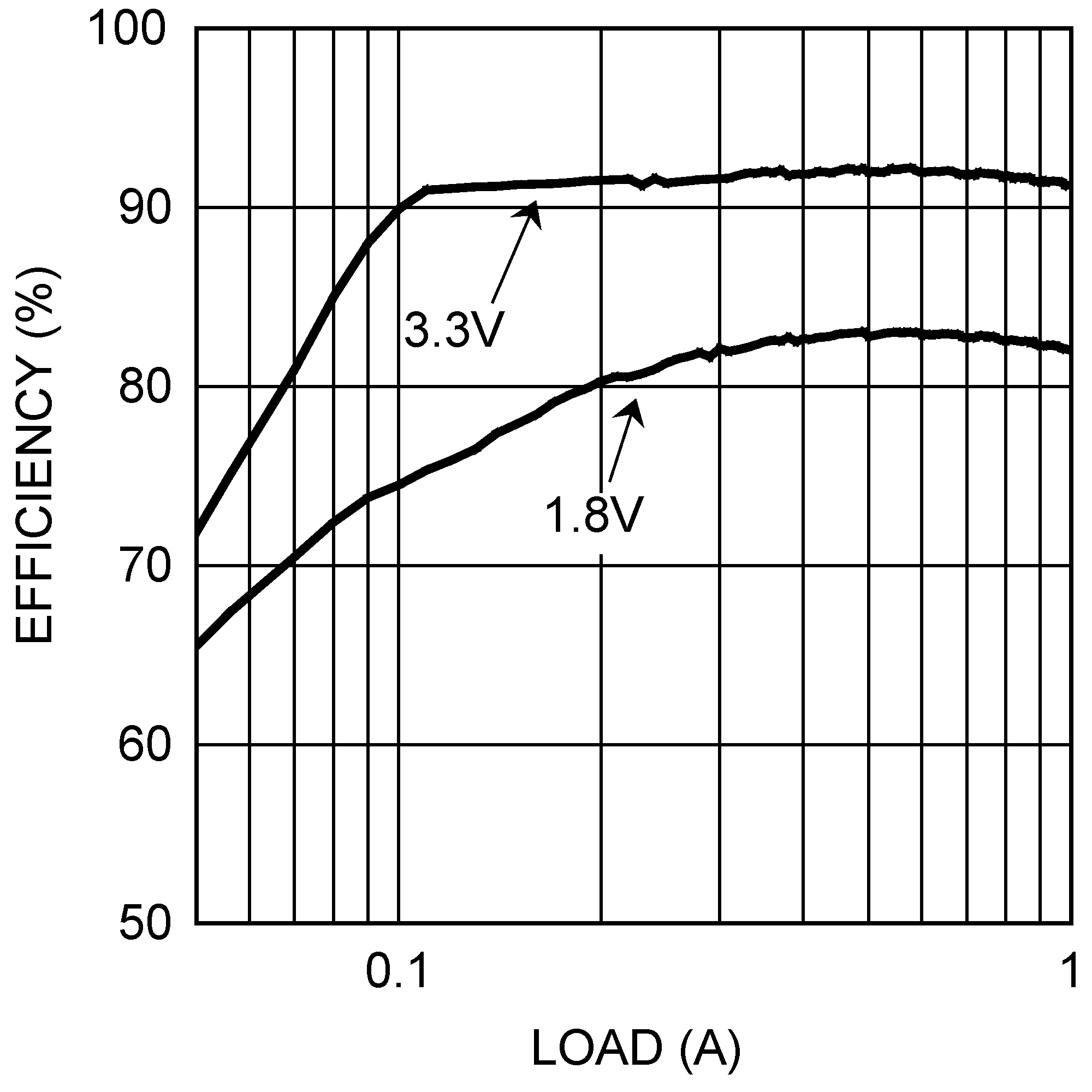
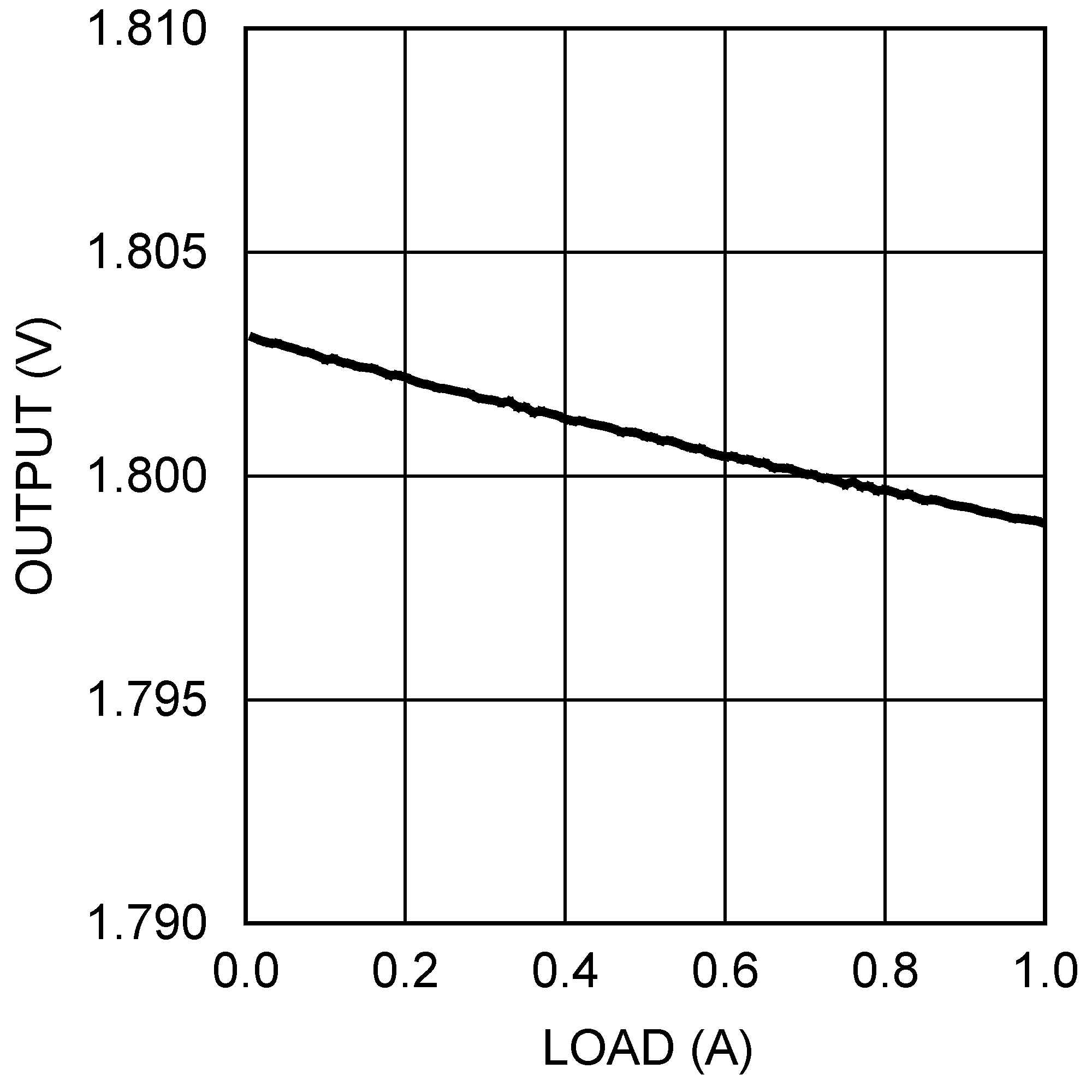
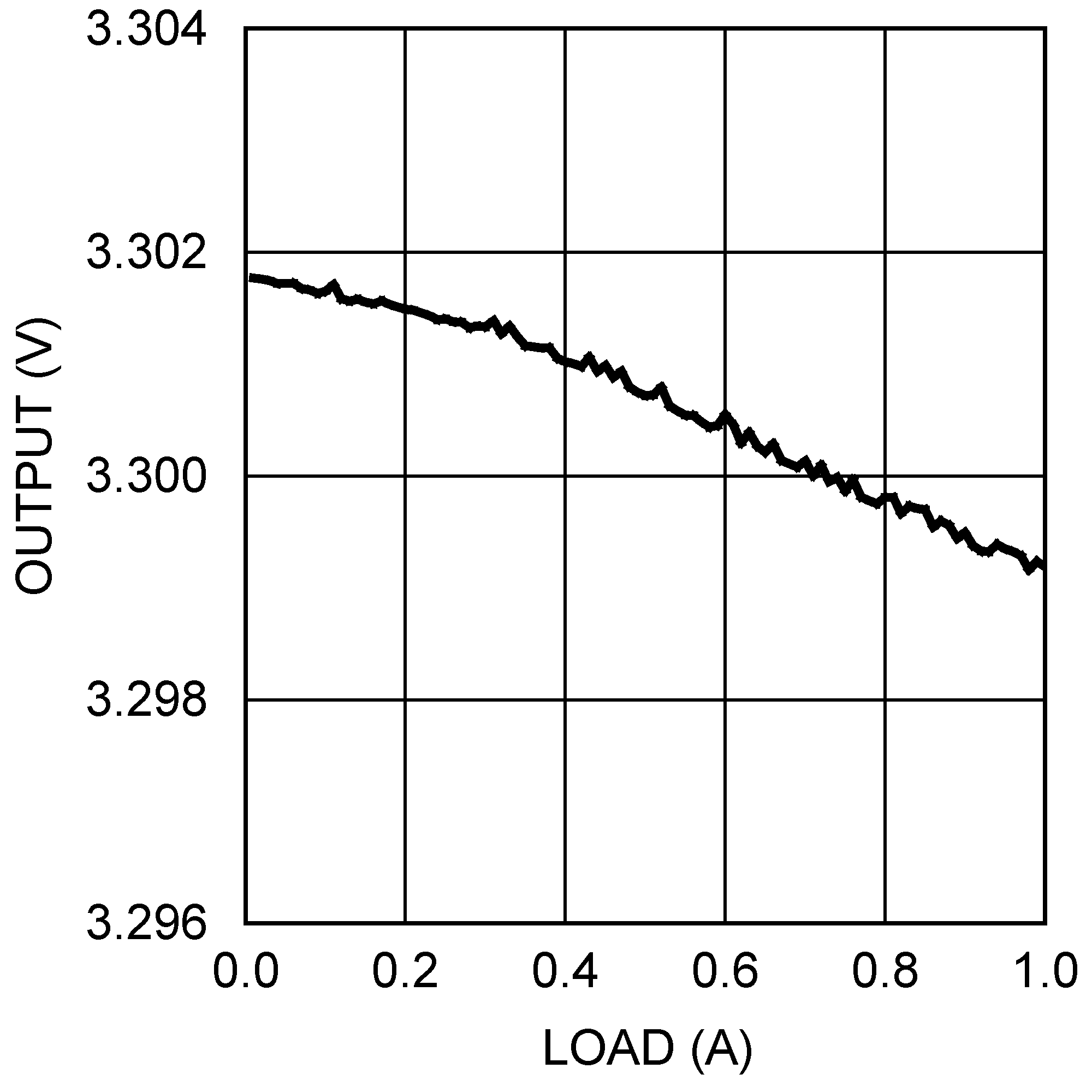
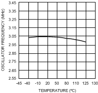
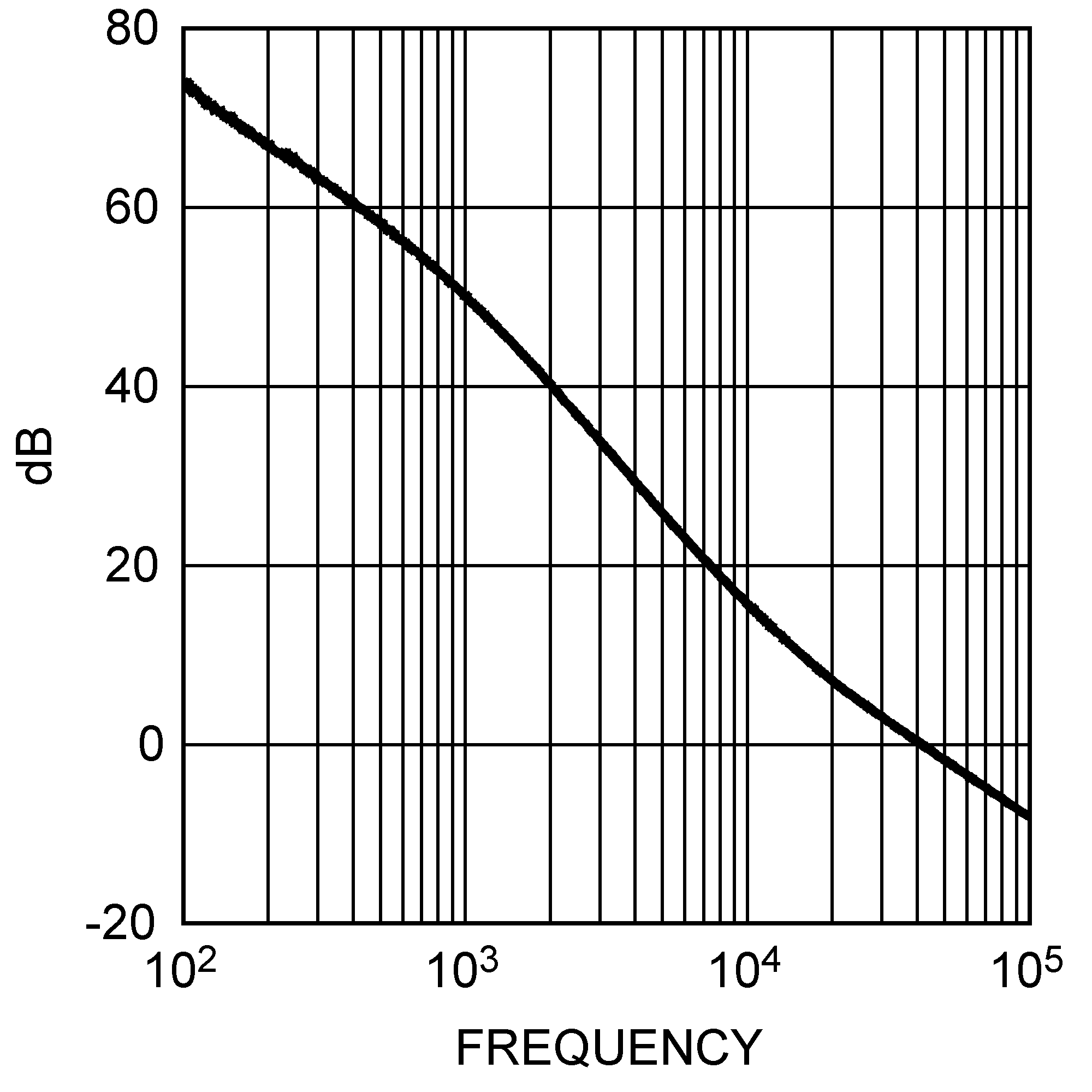
6.7 Typical Characteristics
All curves taken at VIN = 5.0 V with configuration in typical application circuit shown in Application Information section of this data sheet. TJ = 25°C, unless otherwise specified.