SNVS454E August 2006 – December 2014 LM2830 , LM2830-Q1
PRODUCTION DATA.
- 1 Features
- 2 Applications
- 3 Description
- 4 Revision History
- 5 Pin Configuration and Functions
- 6 Specifications
- 7 Detailed Description
-
8 Application and Implementation
- 8.1 Application Information
- 8.2
Typical Applications
- 8.2.1 LM2830X Design Vo = 1.2 V at 1.0A
- 8.2.2 LM2830X Design Vo = 0.6 V at 1.0-A
- 8.2.3 LM2830X Design Vo = 3.3 V at 1.0-A
- 8.2.4 LM2830Z Design Vo = 3.3 V at 1.0-A
- 8.2.5 LM2830Z Design Vo = 1.2 V at 1.0-A
- 8.2.6 LM2830X Dual Converters With Delayed Enabled Design
- 8.2.7 LM2830X Buck Converter and Voltage Double Circuit With LDO Follower
- 9 Power Supply Recommendations
- 10Layout
- 11Device and Documentation Support
- 12Mechanical, Packaging, and Orderable Information
8 Application and Implementation
NOTE
Information in the following applications sections is not part of the TI component specification, and TI does not warrant its accuracy or completeness. TI’s customers are responsible for determining suitability of components for their purposes. Customers should validate and test their design implementation to confirm system functionality.
8.1 Application Information
The device operates with input voltage in the range of 3.3 V to 5.5 V and provide regulated output voltage up to 1 A of continuous DC load. This device is optimized for high efficiency operation with minimum number of external components. Also, high switching frequency allows use of small surface-mount components enabling very small solution size. For component selection, see Detailed Design Procedure.
8.2 Typical Applications
8.2.1 LM2830X Design Vo = 1.2 V at 1.0A
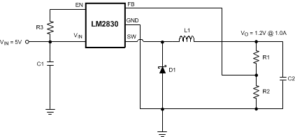 Figure 19. LM2830X (1.6 MHz): Vin = 5 V, Vo = 1.2 V at 1.0-A Schematic
8.2.1.1 Design Requirements
This device must be able to operate at any voltage within input voltage range.
Load Current must be defined to properly size the inductor, input and output capacitors. Inductor should be able to handle full expected load current as well as the peak current generated during load transients and start up. Inrush current at startup will depend on the output capacitor selection. More details are provided in Detailed Design Procedure.
Device has an enable (EN) pin that is used to enable and disable the device. This pin is active high and should not be left floating in application.
8.2.1.2 Detailed Design Procedure
Table 1. Bill of Materials
| PART ID | PART VALUE | MANUFACTURER | PART NUMBER |
|---|---|---|---|
| U1 | 1.0-A Buck Regulator | TI | LM2830X |
| C1, Input Cap | 22 µF, 6.3 V, X5R | TDK | C3216X5ROJ226M |
| C2, Output Cap | 22 µF, 6.3 V, X5R | TDK | C3216X5ROJ226M |
| D1, Catch Diode | 0.3 Vf Schottky 1.5 A, 30 VR | TOSHIBA | CRS08 |
| L1 | 3.3 µH, 1.3 A | Coilcraft | ME3220-332 |
| R2 | 15.0 kΩ, 1% | Vishay | CRCW08051502F |
| R1 | 15.0 kΩ, 1% | Vishay | CRCW08051502F |
| R3 | 100 kΩ, 1% | Vishay | CRCW08051003F |
8.2.1.2.1 Inductor Selection
The Duty Cycle (D) can be approximated quickly using the ratio of output voltage (VO) to input voltage (VIN):

The catch diode (D1) forward voltage drop and the voltage drop across the internal PMOS must be included to calculate a more accurate duty cycle. Calculate D by using the following formula:

VSW can be approximated by:
The diode forward drop (VD) can range from 0.3 V to 0.7 V depending on the quality of the diode. The lower the VD, the higher the operating efficiency of the converter. The inductor value determines the output ripple current. Lower inductor values decrease the size of the inductor, but increase the output ripple current. An increase in the inductor value will decrease the output ripple current.
One must ensure that the minimum current limit (1.2 A) is not exceeded, so the peak current in the inductor must be calculated. The peak current (ILPK) in the inductor is calculated by:
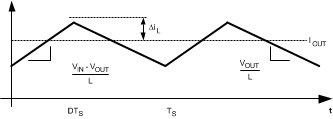 Figure 20. Inductor Current

In general,
If ΔiL = 20% of 1 A, the peak current in the inductor will be 1.2 A. The minimum ensured current limit over all operating conditions is 1.2 A. One can either reduce ΔiL, or make the engineering judgment that zero margin will be safe enough. The typical current limit is 1.75 A.
The LM2830 device operates at frequencies allowing the use of ceramic output capacitors without compromising transient response. Ceramic capacitors allow higher inductor ripple without significantly increasing output ripple. See the Output Capacitor for more details on calculating output voltage ripple. Now that the ripple current is determined, the inductance is calculated by:
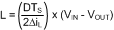
where
- Ts = 1/fs
When selecting an inductor, make sure that it is capable of supporting the peak output current without saturating. Inductor saturation will result in a sudden reduction in inductance and prevent the regulator from operating correctly. Because of the speed of the internal current limit, it is necessary to specify the peak current of the inductor only required maximum output current. For example, if the designed maximum output current is 1.0 A and the peak current is 1.25 A, then the inductor should be specified with a saturation current limit of > 1.25 A. There is no need to specify the saturation or peak current of the inductor at the 1.75-A typical switch current limit. The difference in inductor size is a factor of 5. Because of the operating frequency of the LM2830 device, ferrite based inductors are preferred to minimize core losses. This presents little restriction because the variety of ferrite-based inductors is huge. Lastly, inductors with lower series resistance (RDCR) will provide better operating efficiency.
8.2.1.2.2 Input Capacitor
An input capacitor is necessary to ensure that VIN does not drop excessively during switching transients. The primary specifications of the input capacitor are capacitance, voltage, RMS current rating, and ESL (Equivalent Series Inductance). The recommended input capacitance is 22 µF. The input voltage rating is specifically stated by the capacitor manufacturer. Make sure to check any recommended deratings and also verify if there is any significant change in capacitance at the operating input voltage and the operating temperature. The input capacitor maximum RMS input current rating (IRMS-IN) must be greater than:
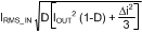
Neglecting inductor ripple simplifies the above equation to:

From Equation 9, it can be shown that maximum RMS capacitor current occurs when D = 0.5. Always calculate the RMS at the point where the duty cycle D is closest to 0.5. The ESL of an input capacitor is usually determined by the effective cross sectional area of the current path. A large leaded capacitor will have high ESL and a 0805 ceramic chip capacitor will have very low ESL. At the operating frequencies of the LM2830 device, leaded capacitors may have an ESL so large that the resulting impedance (2πfL) will be higher than that required to provide stable operation. As a result, surface-mount capacitors are strongly recommended.
Sanyo POSCAP, Tantalum or Niobium, Panasonic SP, and multilayer ceramic capacitors (MLCC) are all good choices for both input and output capacitors and have very low ESL. For MLCCs it is recommended to use X7R or X5R type capacitors due to their tolerance and temperature characteristics. Consult the capacitor manufacturer data sheets to see how rated capacitance varies over operating conditions.
8.2.1.2.3 Output Capacitor
The output capacitor is selected based upon the desired output ripple and transient response. The initial current of a load transient is provided mainly by the output capacitor. The output ripple of the converter is:
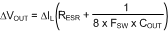
When using MLCCs, the ESR is typically so low that the capacitive ripple may dominate. When this occurs, the output ripple will be approximately sinusoidal and 90° phase shifted from the switching action. Given the availability and quality of MLCCs and the expected output voltage of designs using the LM2830 device, there is really no need to review any other capacitor technologies. Another benefit of ceramic capacitors is their ability to bypass high frequency noise. A certain amount of switching edge noise will couple through parasitic capacitances in the inductor to the output. A ceramic capacitor will bypass this noise while a tantalum will not. Because the output capacitor is one of the two external components that control the stability of the regulator control loop, most applications will require a minimum of 22 µF of output capacitance. Capacitance often, but not always, can be increased significantly with little detriment to the regulator stability. Like the input capacitor, recommended multilayer ceramic capacitors are X7R or X5R types.
8.2.1.2.4 Catch Diode
The catch diode (D1) conducts during the switch off-time. A Schottky diode is recommended for its fast switching times and low forward voltage drop. The catch diode should be chosen so that its current rating is greater than:
The reverse breakdown rating of the diode must be at least the maximum input voltage plus appropriate margin. To improve efficiency, choose a Schottky diode with a low forward voltage drop.
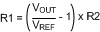
8.2.1.2.5 Output Voltage
The output voltage is set using Equation 12, where R2 is connected between the FB pin and GND, and R1 is connected between VO and the FB pin. A good value for R2 is 10 kΩ. When designing a unity gain converter (Vo = 0.6 V), R1 should be between 0 Ω and 100 Ω, and R2 should be equal or greater than 10 kΩ.
8.2.1.2.6 Calculating Efficiency, and Junction Temperature
The complete LM2830 DC-DC converter efficiency can be calculated in the following manner.

Or

Calculations for determining the most significant power losses are shown below. Other losses totaling less than 2% are not discussed.
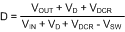
Power loss (PLOSS) is the sum of two basic types of losses in the converter: switching and conduction. Conduction losses usually dominate at higher output loads, whereas switching losses remain relatively fixed and dominate at lower output loads. The first step in determining the losses is to calculate the duty cycle (D):
VSW is the voltage drop across the internal PFET when it is on, and is equal to:
VD is the forward voltage drop across the Schottky catch diode. It can be obtained from the diode manufacturer's Electrical Characteristics section. If the voltage drop across the inductor (VDCR) is accounted for, the equation becomes:
The conduction losses in the free-wheeling Schottky diode are calculated as follows:
Often this is the single most significant power loss in the circuit. Care should be taken to choose a Schottky diode that has a low forward voltage drop.
Another significant external power loss is the conduction loss in the output inductor. The equation can be simplified to:
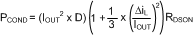
The conduction loss of the LC2830 device is mainly associated with the internal PFET:
If the inductor ripple current is fairly small, the conduction losses can be simplified to:
Switching losses are also associated with the internal PFET. They occur during the switch on and off transition periods, where voltages and currents overlap resulting in power loss. The simplest means to determine this loss is to empirically measuring the rise and fall times (10% to 90%) of the switch at the switch node.
Switching Power Loss is calculated as follows:
Another loss is the power required for operation of the internal circuitry:
IQ is the quiescent operating current, and is typically around 3.3 mA for the 1.6-MHz frequency option.
Table 2 lists typical application power losses.
Table 2. Power Loss Tabulation
| Design Parameter | Value | Design Parameter | Value |
|---|---|---|---|
| VIN | 5.0 V | ||
| VOUT | 3.3 V | POUT | 3.3 W |
| IOUT | 1.0A | ||
| VD | 0.45 V | PDIODE | 150 mW |
| FSW | 1.6 MHz | ||
| IQ | 3.3 mA | PQ | 17 mW |
| TRISE | 4 nS | PSWR | 6 mW |
| TFALL | 4 nS | PSWF | 6 mW |
| RDS(ON) | 150 mΩ | PCOND | 100 mW |
| INDDCR | 70 mΩ | PIND | 70 mW |
| D | 0.667 | PLOSS | 345 mW |
| η | 88% | PINTERNAL | 125 mW |
8.2.2 LM2830X Design Vo = 0.6 V at 1.0-A
Figure 23 shows typical application circuit for step-down solution from VIN=5 to VOUT=0.6 V, 1.0-A load current.
 Figure 23. LM2830X (1.6 MHz): Vin = 5 V, Vo = 0.6 V at 1.0-A Schematic
Table 3. Bill of Materials
| PART ID | PART VALUE | MANUFACTURER | PART NUMBER |
|---|---|---|---|
| U1 | 1.0-A Buck Regulator | TI | LM2830X |
| C1, Input Cap | 22 µF, 6.3 V, X5R | TDK | C3216X5ROJ226M |
| C2, Output Cap | 22 µF, 6.3 V, X5R | TDK | C3216X5ROJ226M |
| D1, Catch Diode | 0.3 Vf Schottky 1.5 A, 30 VR | TOSHIBA | CRS08 |
| L1 | 3.3 µH, 1.3 A | Coilcraft | ME3220-332 |
| R2 | 10.0 kΩ, 1% | Vishay | CRCW08051000F |
| R1 | 0 Ω | ||
| R3 | 100 kΩ, 1% | Vishay | CRCW08051003F |
8.2.3 LM2830X Design Vo = 3.3 V at 1.0-A
Figure 24 shows typical application circuit for step down solution from VIN=5 to VOUT=3.3 V, 1.0-A load current.
 Figure 24. LM2830X (1.6 MHz): Vin = 5 V, Vo = 3.3 V at 1.0-A Schematic
Table 4. Bill of Materials
| PART ID | PART VALUE | MANUFACTURER | PART NUMBER |
|---|---|---|---|
| U1 | 1.0-A Buck Regulator | TI | LM2830X |
| C1, Input Cap | 22 µF, 6.3 V, X5R | TDK | C3216X5ROJ226M |
| C2, Output Cap | 22 µF, 6.3 V, X5R | TDK | C3216X5ROJ226M |
| D1, Catch Diode | 0.3 Vf Schottky 1.5 A, 30 VR | TOSHIBA | CRS08 |
| L1 | 2.2 µH, 1.8 A | Coilcraft | ME3220-222 |
| R2 | 10.0 kΩ, 1% | Vishay | CRCW08051002F |
| R1 | 45.3 kΩ, 1% | Vishay | CRCW08054532F |
| R3 | 100 kΩ, 1% | Vishay | CRCW08051003F |
8.2.4 LM2830Z Design Vo = 3.3 V at 1.0-A
Figure 25 shows typical application circuit for step down solution from VIN=5 to VOUT=3.3 V, 1.0-A load current when using device version with higher switching frequency.
Figure 25. LM2830Z (3 MHz): Vin = 5 V, Vo = 3.3 V at 1.0-A Schematic
Table 5. Bill of Materials
| PART ID | PART VALUE | MANUFACTURER | PART NUMBER |
|---|---|---|---|
| U1 | 1.0-A Buck Regulator | TI | LM2830Z |
| C1, Input Cap | 22 µF, 6.3 V, X5R | TDK | C3216X5ROJ226M |
| C2, Output Cap | 22 µF, 6.3 V, X5R | TDK | C3216X5ROJ226M |
| D1, Catch Diode | 0.3 Vf Schottky 1.5 A, 30VR | TOSHIBA | CRS08 |
| L1 | 1.6 µH, 2.0 A | TDK | VLCF4018T-1R6N1R7-2 |
| R2 | 10.0 kΩ, 1% | Vishay | CRCW08051002F |
| R1 | 45.3 kΩ, 1% | Vishay | CRCW08054532F |
| R3 | 100 kΩ, 1% | Vishay | CRCW08051003F |
8.2.5 LM2830Z Design Vo = 1.2 V at 1.0-A
Figure 26 shows a typical application circuit for step down solution from VIN=5 to VOUT=1.2 V, 1.0-A load current when using device version with higher switching frequency.
Figure 26. LM2830Z (3 MHz): Vin = 5 V, Vo = 1.2 V at 1.0-A Schematic
Table 6. Bill of Materials
| PART ID | PART VALUE | MANUFACTURER | PART NUMBER |
|---|---|---|---|
| U1 | 1.0-A Buck Regulator | TI | LM2830Z |
| C1, Input Cap | 22 µF, 6.3 V, X5R | TDK | C3216X5ROJ226M |
| C2, Output Cap | 22 µF, 6.3 V, X5R | TDK | C3216X5ROJ226M |
| D1, Catch Diode | 0.3Vf Schottky 1.5 A, 30VR | TOSHIBA | CRS08 |
| L1 | 1.6 µH, 2.0 A | TDK | VLCF4018T-1R6N1R7-2 |
| R2 | 10.0 kΩ, 1% | Vishay | CRCW08051002F |
| R1 | 10.0 kΩ, 1% | Vishay | CRCW08051002F |
| R3 | 100 kΩ, 1% | Vishay | CRCW08051003F |
8.2.6 LM2830X Dual Converters With Delayed Enabled Design
Figure 27 shows proposed solution with two LM2830 devices. Output of device on top (3.3-V output) is used to control the enable pin of the lower device, thus ensuring that the second device (1.2-V output) can not turn on before the output of first device (3.3-V in this example) reaches steady state. Additionally, small POR supervisory (LP3470) circuit is used to monitor enable voltage for lower device. The RESET pin on POR circuit is open drain and requires typically 20-kΩ pullup resistor to the monitored voltage.
 Figure 27. LM2830X (1.6 MHz): Vin = 5 V, Vo = 1.2 V at 1.0 A and 3.3 V at 1.0-A Schematic
Table 7. Bill of Materials
| PART ID | PART VALUE | MANUFACTURER | PART NUMBER |
|---|---|---|---|
| U1, U2 | 1.0-A Buck Regulator | TI | LM2830X |
| U3 | Power on Reset | TI | LP3470M5X-3.08 |
| C1, C3 Input Cap | 22 µF, 6.3 V, X5R | TDK | C3216X5ROJ226M |
| C2, C4 Output Cap | 22 µF, 6.3 V, X5R | TDK | C3216X5ROJ226M |
| C7 | Trr delay capacitor | TDK | |
| D1, D2 Catch Diode | 0.3 Vf Schottky 1.5 A, 30 VR | TOSHIBA | CRS08 |
| L1, L2 | 3.3 µH, 1.3 A | Coilcraft | ME3220-332 |
| R2, R4, R5 | 10.0 kΩ, 1% | Vishay | CRCW08051002F |
| R1, R6 | 45.3 kΩ, 1% | Vishay | CRCW08054532F |
| R3 | 100 kΩ, 1% | Vishay | CRCW08051003F |
8.2.7 LM2830X Buck Converter and Voltage Double Circuit With LDO Follower
Figure 28 shows an example where the LM2830 device is used to provide regulated output voltage (3.3 V) as well as input voltage for an LDO, effectively providing solution with two output voltages.
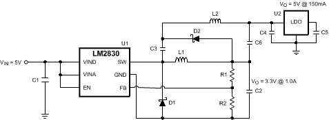 Figure 28. LM2830X (1.6 MHz): Vin = 5 V, Vo = 3.3 V at 1.0 A and LP2986-5.0 at 150-mA Schematic
Table 8. Bill of Materials
| PART ID | PART VALUE | MANUFACTURER | PART NUMBER |
|---|---|---|---|
| U1 | 1.0-A Buck Regulator | TI | LM2830X |
| U2 | 200-mA LDO | TI | LP2986-5.0 |
| C1, Input Cap | 22 µF, 6.3 V, X5R | TDK | C3216X5ROJ226M |
| C2, Output Cap | 22 µF, 6.3 V, X5R | TDK | C3216X5ROJ226M |
| C3 – C6 | 2.2 µF, 6.3 V, X5R | TDK | C1608X5R0J225M |
| D1, Catch Diode | 0.3 Vf Schottky 1.5 A, 30 VR | TOSHIBA | CRS08 |
| D2 | 0.4 Vf Schottky 20 VR, 500 mA | ON Semi | MBR0520 |
| L2 | 10 µH, 800 mA | CoilCraft | ME3220-103 |
| L1 | 3.3 µH, 2.2 A | TDK | VLCF5020T-3R3N2R0-1 |
| R2 | 45.3 kΩ, 1% | Vishay | CRCW08054532F |
| R1 | 10.0 kΩ, 1% | Vishay | CRCW08051002F |