SNVS002E January 1999 – October 2014 LM2662 , LM2663
PRODUCTION DATA.
- 1 Features
- 2 Applications
- 3 Description
- 4 Revision History
- 5 Pin Configuration and Functions
- 6 Specifications
- 7 Parameter Measurement Information
- 8 Detailed Description
- 9 Application and Implementation
- 10Power Supply Recommendations
- 11Layout
- 12Device and Documentation Support
- 13Mechanical, Packaging, and Orderable Information
6 Specifications
6.1 Absolute Maximum Ratings
over operating free-air temperature range (unless otherwise noted)(1)(2)| MIN | MAX | UNIT | |
|---|---|---|---|
| Supply voltage (V+ to GND, or GND to OUT) | 6 | V | |
| LV | (OUT − 0.3 V) | (GND + 3 V) | |
| FC, OSC, SD | The least negative of (OUT − 0.3 V) or (V+ − 6 V) to (V+ + 0.3 V) |
||
| V+ and OUT continuous output current | 250 | ||
| Output short-circuit duration to GND(3) | 1 | sec. | |
| Power dissipation (TA = 25°C)(4) | 735 | mW | |
| TJ max(4) | 150 | °C | |
| Operating ambient temperature | −40 | 85 | |
| Operating junction temperature | −40 | 105 | |
| Lead temperature (soldering, 10 seconds) | 300 | ||
(1) Stresses beyond those listed under Absolute Maximum Ratings may cause permanent damage to the device. These are stress ratings only, which do not imply functional operation of the device at these or any other conditions beyond those indicated under Recommended Operating Conditions. Exposure to absolute-maximum-rated conditions for extended periods may affect device reliability.
(2) If Military/Aerospace specified devices are required, please contact the Texas Instruments Sales Office/Distributors for availability and specifications.
(3) OUT may be shorted to GND for one second without damage. However, shorting OUT to V+ may damage the device and should be avoided. Also, for temperatures above 85°C, OUT must not be shorted to GND or V+, or device may be damaged.
(4) The maximum allowable power dissipation is calculated by using PDMax = (TJMax − TA)/RθJA, where TJMax is the maximum junction temperature, TA is the ambient temperature, and RθJA is the junction-to-ambient thermal resistance of the specified package.
6.2 Handling Ratings
| MIN | MAX | UNIT | |||
|---|---|---|---|---|---|
| Tstg | Storage temperature range | −65 | 150 | °C | |
| V(ESD) | Electrostatic discharge | Human body model (HBM), per ANSI/ESDA/JEDEC JS-001, all pins(1) | 2000 | V | |
(1) JEDEC document JEP155 states that 500-V HBM allows safe manufacturing with a standard ESD control process.
6.3 Recommended Operating Conditions
over operating free-air temperature range (unless otherwise noted)| MIN | NOM | MAX | UNIT | ||
|---|---|---|---|---|---|
| V+ (supply voltage) | 2.5 | 5.5 | V | ||
| Junction temperature (TJ) | –40 | 105 | °C | ||
| Ambient temperature (TJ) | –40 | 85 | |||
6.4 Thermal Information
| THERMAL METRIC(1) | LM2662 | LM2663 | UNIT | |
|---|---|---|---|---|
| SOIC (D) | ||||
| 8 PINS | ||||
| RθJA | Junction-to-ambient thermal resistance | 170 | 170 | °C/W |
(1) For more information about traditional and new thermal metrics, see the IC Package Thermal Metrics application report, SPRA953.
6.5 Electrical Characteristics
Unless otherwise specified: V+ = 5 V, FC = Open, C1 = C2 = 47 μF.(1)| PARAMETER | TEST CONDITION | MIN(2) | TYP(3) | MAX(2) | UNIT | ||
|---|---|---|---|---|---|---|---|
| V+ | Supply Voltage | RL = 1k | Inverter, LV = Open | 3.5 | 5.5 | V | |
| Inverter, LV = GND | 1.5 | 5.5 | |||||
| Doubler, LV = OUT | 2.5 | 5.5 | |||||
| IQ | Supply Current | No Load | FC = V+ (LM2662) | 1.3 | 4 | mA | |
| LV = Open | SD = Ground (LM2663) | ||||||
| FC = Open | 0.3 | 0.8 | |||||
| ISD | Shutdown Supply Current (LM2663) | 10 | μA | ||||
| VSD | Shutdown Pin Input Voltage (LM2663) | Shutdown Mode | 2 | (4) | V | ||
| Normal Operation | 0.3 | ||||||
| IL | Output Current | 200 | mA | ||||
| ROUT | Output Resistance(5) | IL = 200 mA | 3.5 | 7 | Ω | ||
| fOSC | Oscillator Frequency(6) | OSC = Open | FC = Open | 7 | 20 | kHz | |
| FC = V+ | 55 | 150 | |||||
| fSW | Switching Frequency(7) | OSC = Open | FC = Open | 3.5 | 10 | kHz | |
| FC = V+ | 27.5 | 75 | |||||
| IOSC | OSC Input Current | FC = Open | ±2 | μA | |||
| FC = V+ | ±10 | ||||||
| PEFF | Power Efficiency | RL (500) between V+ and OUT | 90% | 96% | |||
| IL = 200 mA to GND | 86% | ||||||
| VOEFF | Voltage Conversion Efficiency | No Load | 99% | 99.96% | |||
(1) In the test circuit, capacitors C1 and C2 are 47-μF, 0.2-Ω maximum ESR capacitors. Capacitors with higher ESR will increase output resistance, reduce output voltage and efficiency.
(2) –40°C to 105°C
(3) TJ = 25°C
(4) In doubling mode, when Vout > 5 V, minimum input high for shutdown equals Vout − 3 V.
(5) Specified output resistance includes internal switch resistance and capacitor ESR.
(6) For LM2663, the oscillator frequency is 150 kHz.
(7) The output switches operate at one half of the oscillator frequency, ƒOSC = 2ƒSW.
6.6 Typical Performance Characteristics
(Circuit of Figure 14 and Figure 15)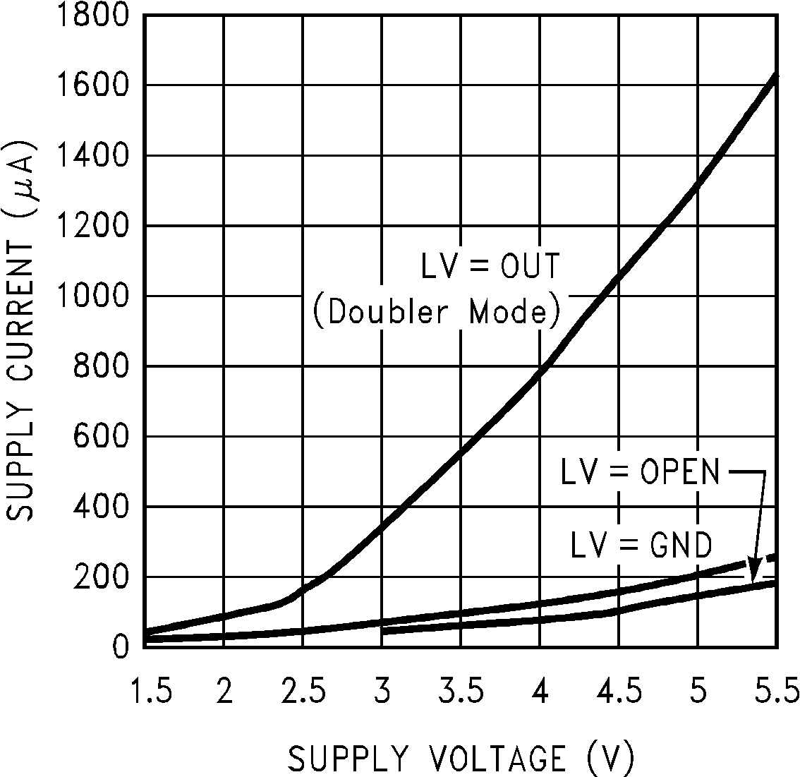 Figure 1. Supply Current vs Supply Voltage
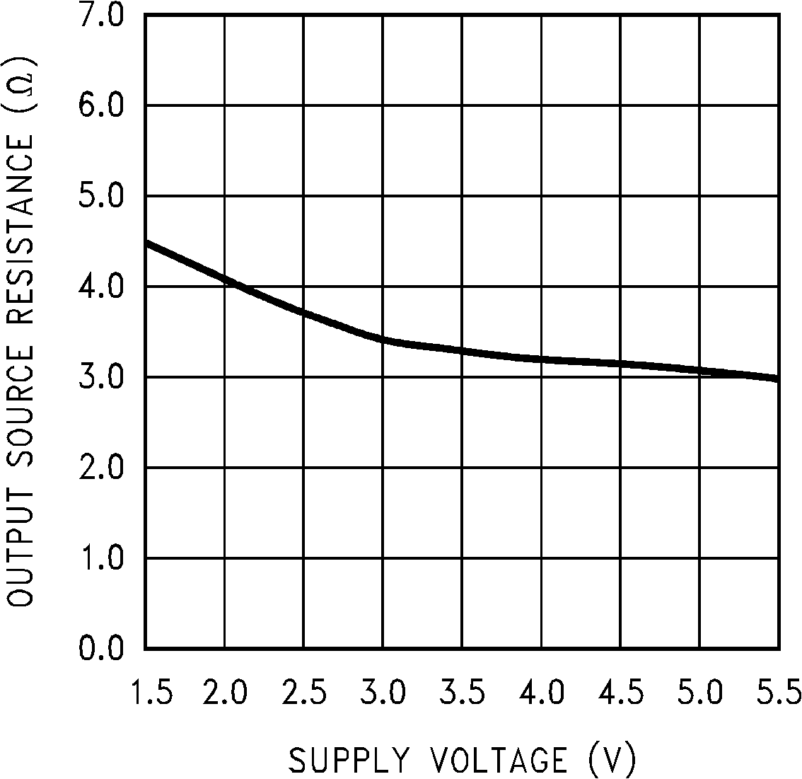 Figure 3. Output Source Resistance vs Supply Voltage
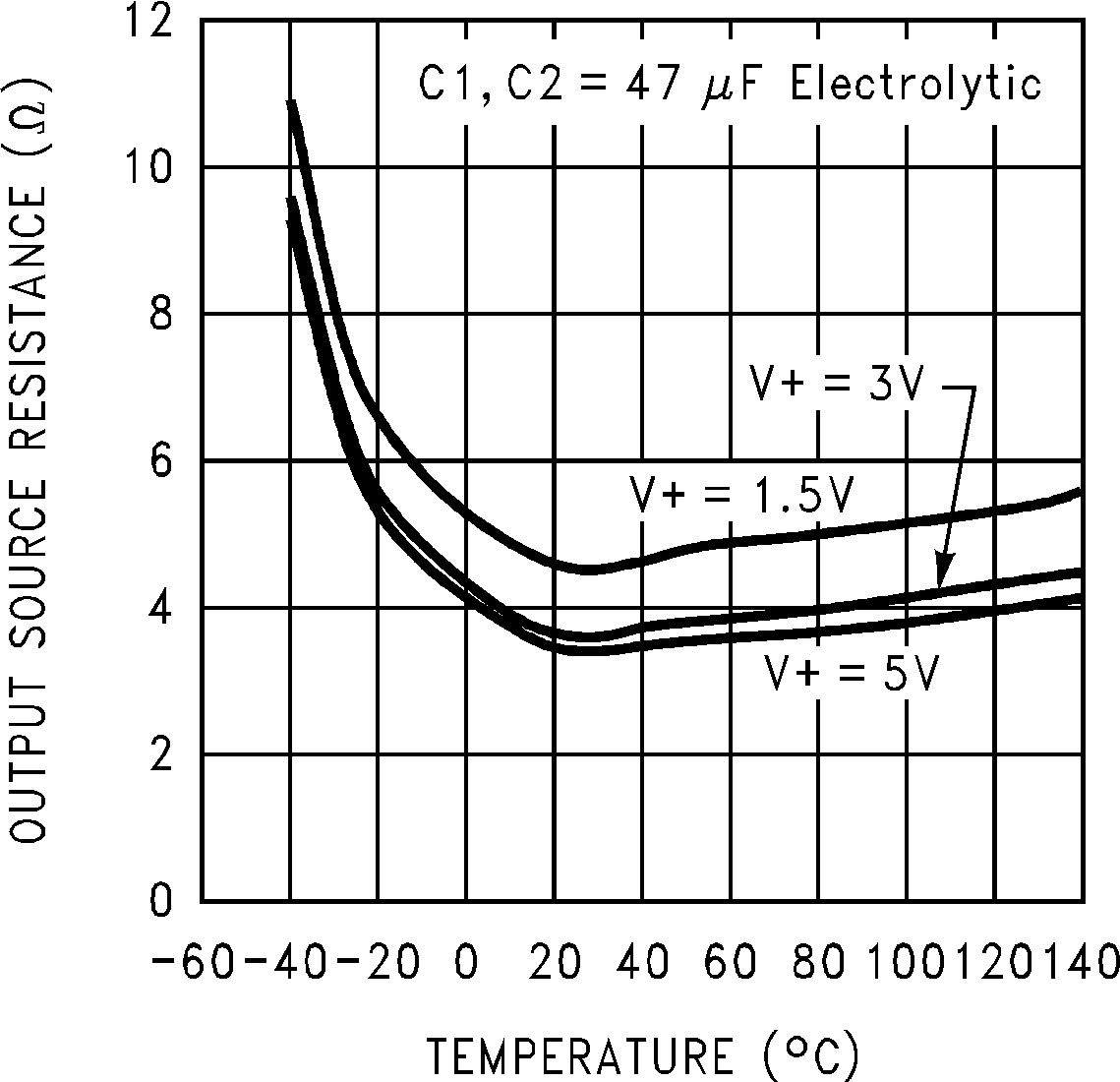 Figure 5. Output Source Resistance vs Temperature
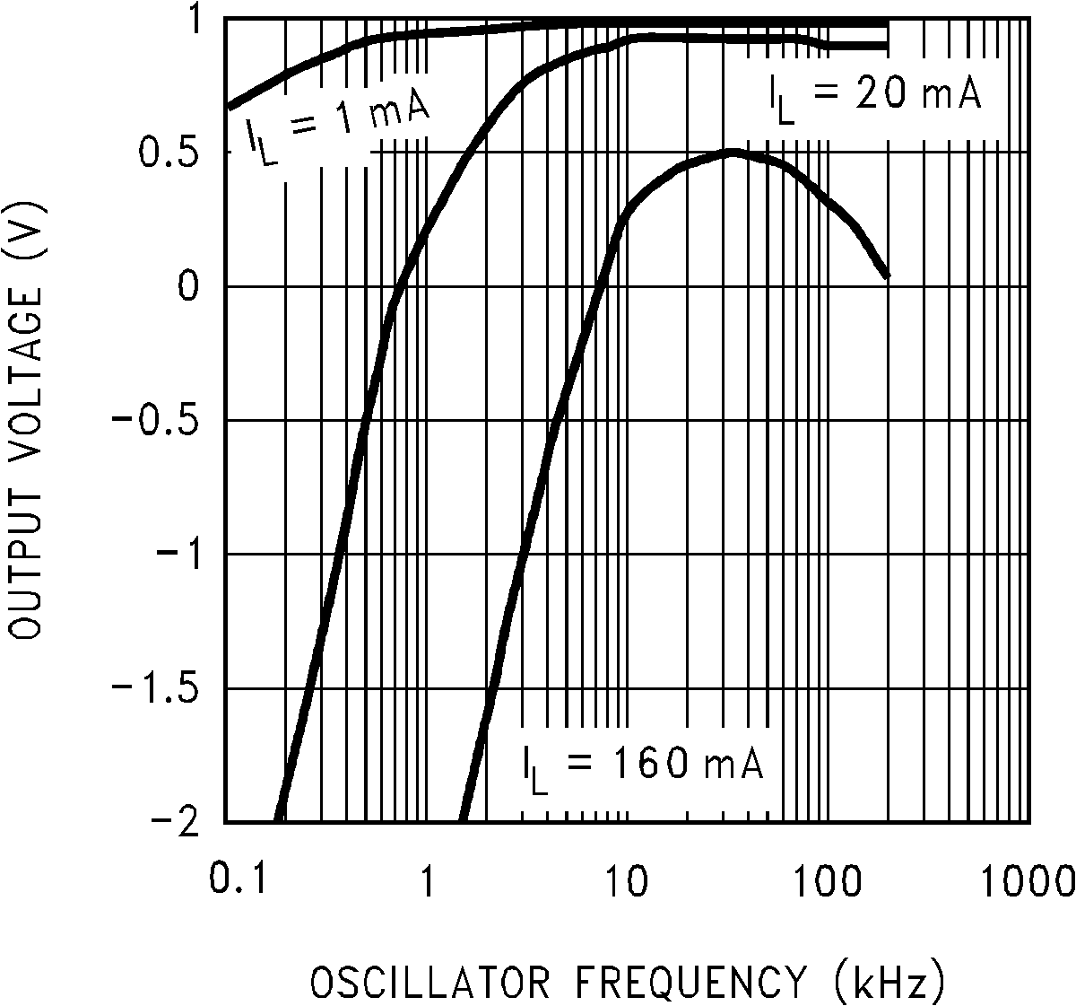 Figure 7. Output Voltage vs Oscillator Frequency
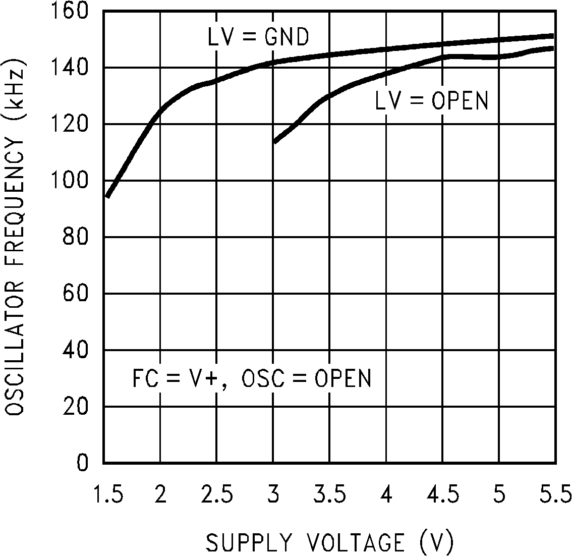 Figure 9. Oscillator Frequency vs Supply Voltage
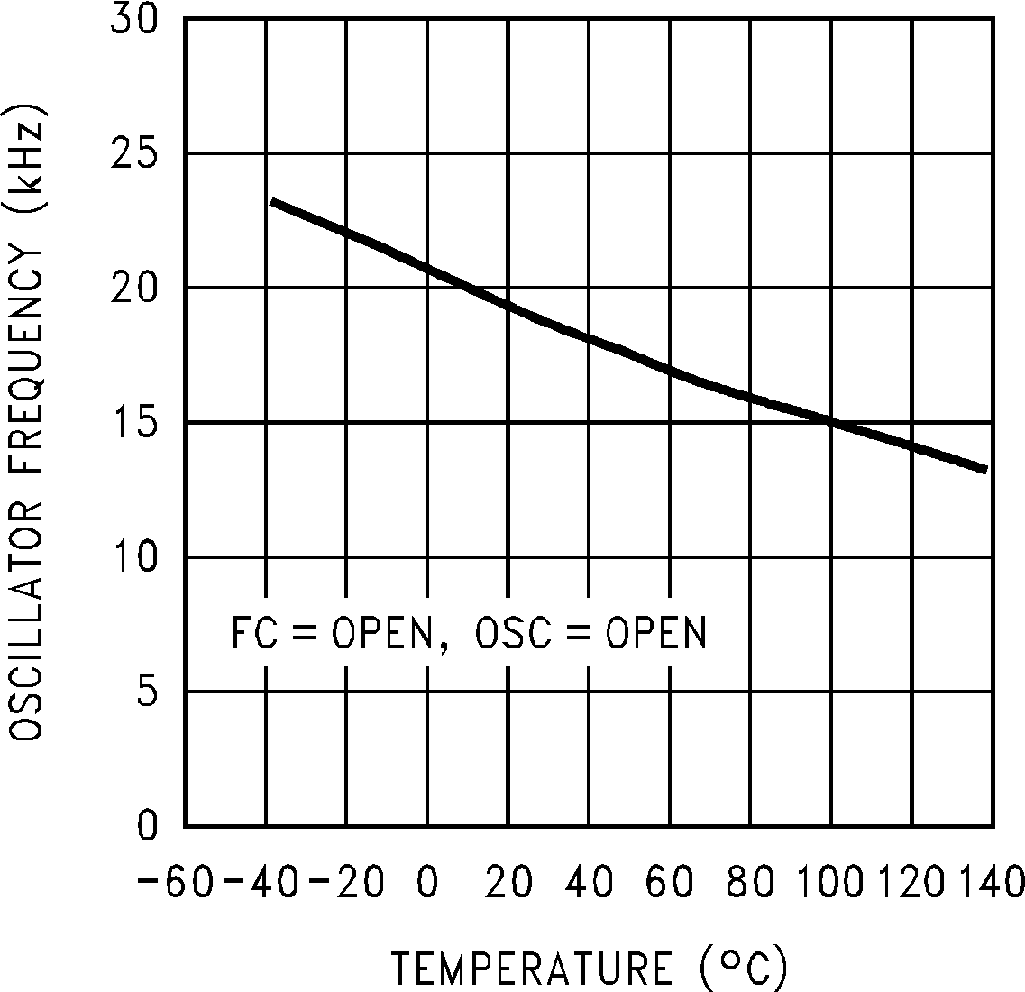 Figure 11. Oscillator Frequency vs Temperatur
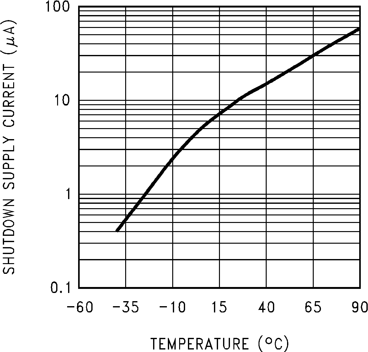 Figure 13. Shutdown Supply Current vs Temperature (LM2663 Only)
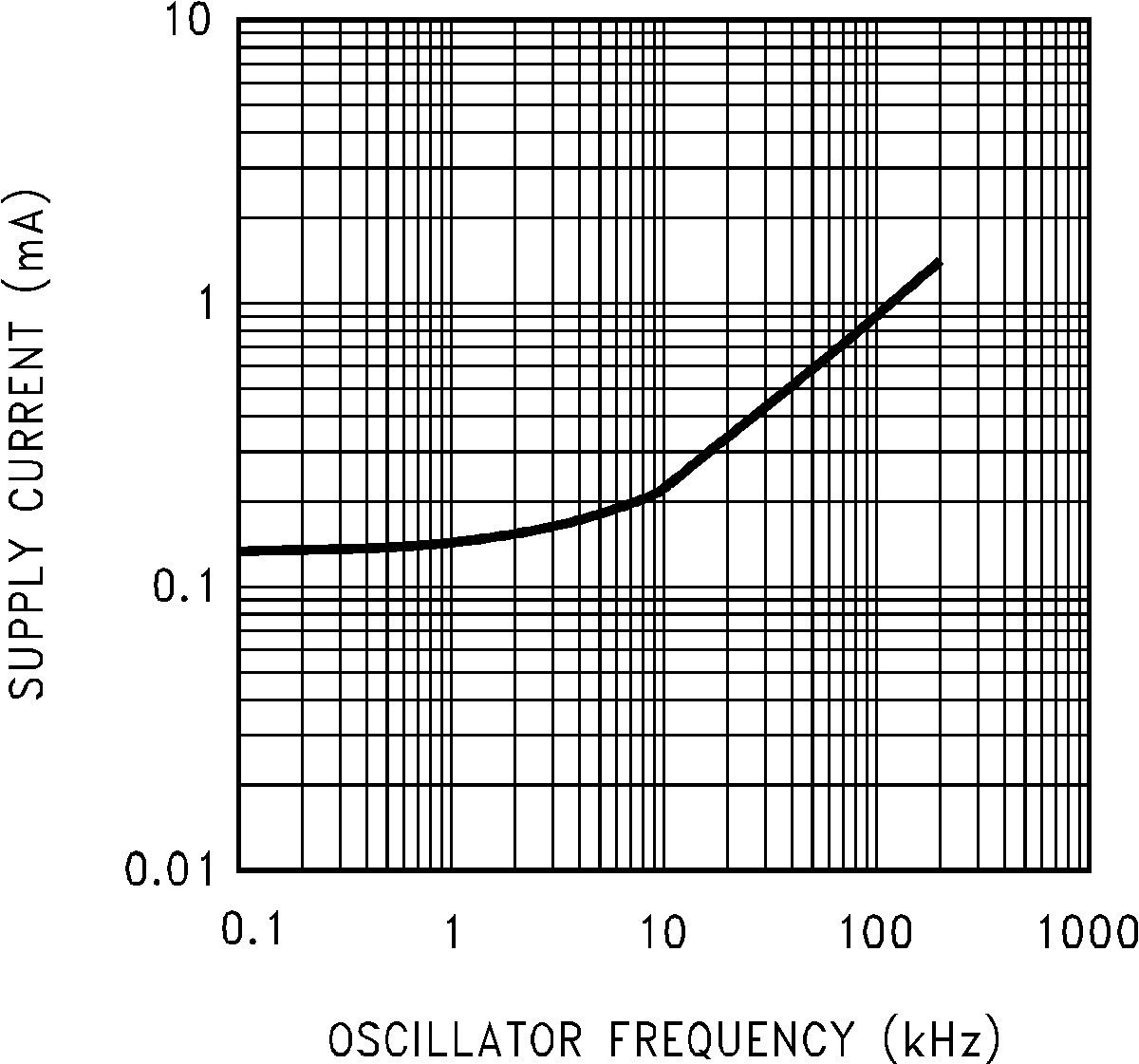 Figure 2. Supply Current vs Oscillator Frequency
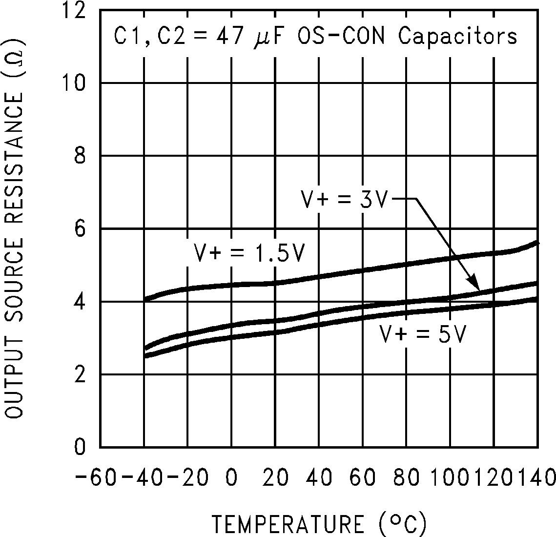 Figure 4. Output Source Resistance vs Temperature
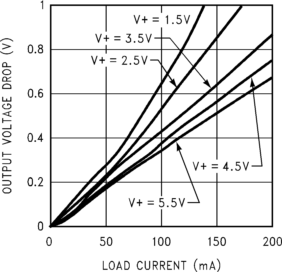 Figure 6. Output Voltage Drop vs Load Current
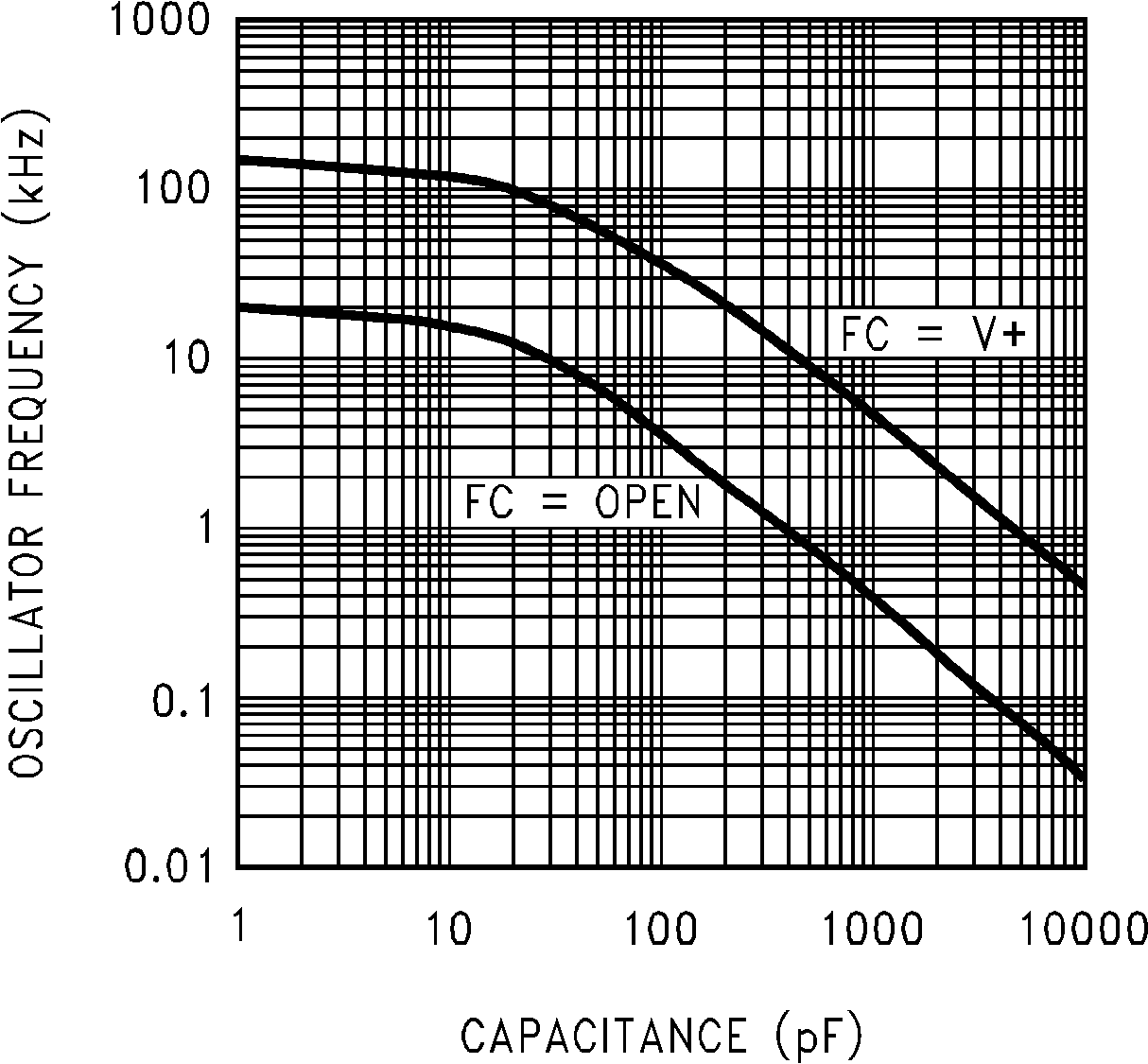 Figure 8. Oscillator Frequency vs External Capacitance
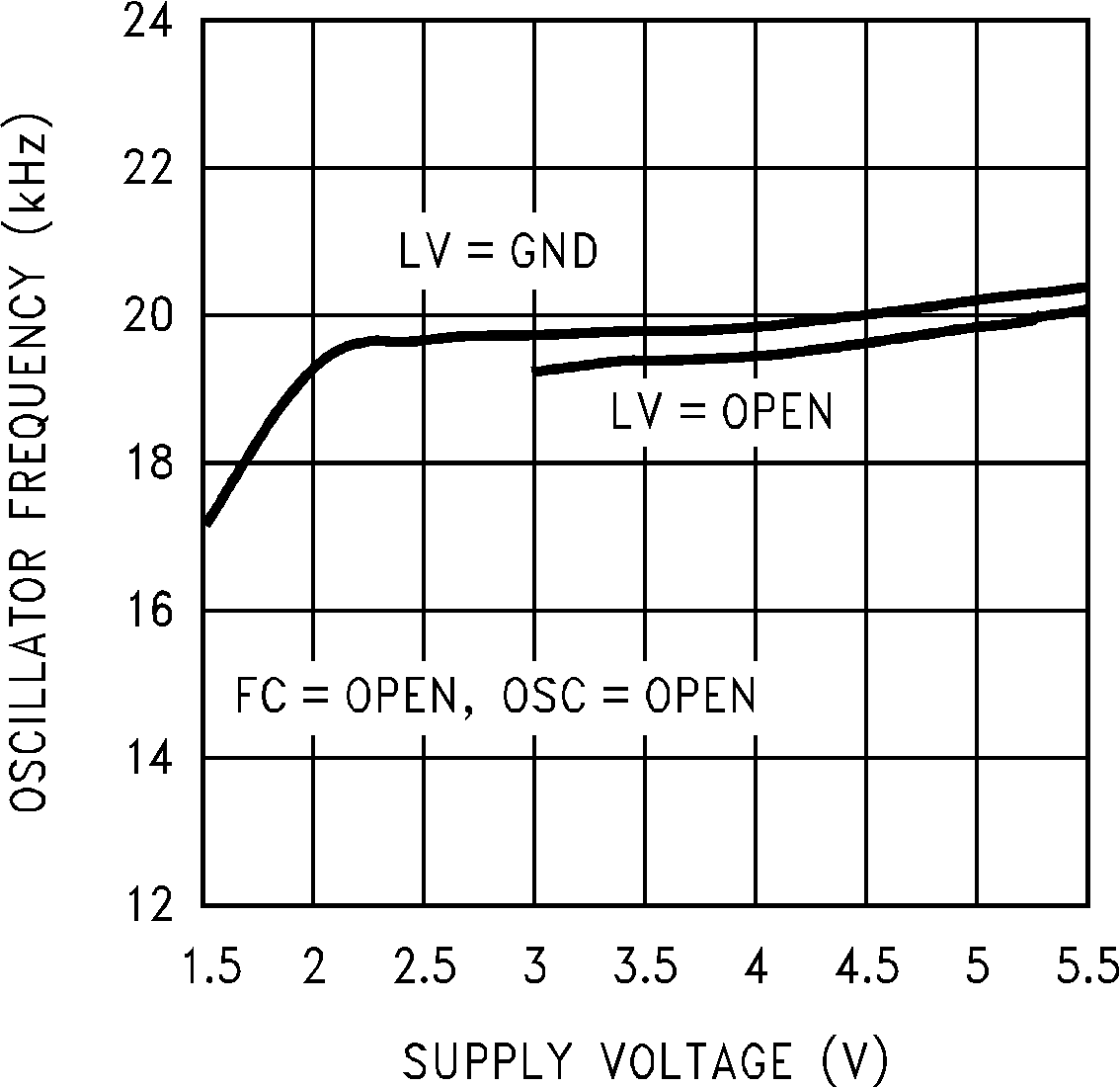 Figure 10. Oscillator Frequency vs Supply Voltage
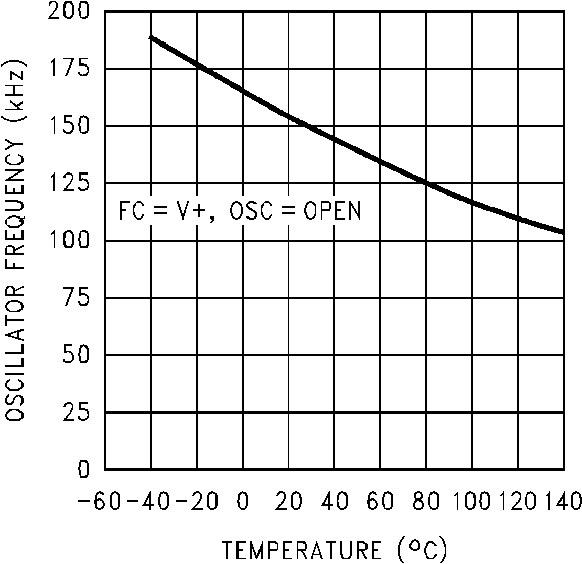 Figure 12. Oscillator Frequency vs Temperature