SNVS002E January 1999 – October 2014 LM2662 , LM2663
PRODUCTION DATA.
- 1 Features
- 2 Applications
- 3 Description
- 4 Revision History
- 5 Pin Configuration and Functions
- 6 Specifications
- 7 Parameter Measurement Information
- 8 Detailed Description
- 9 Application and Implementation
- 10Power Supply Recommendations
- 11Layout
- 12Device and Documentation Support
- 13Mechanical, Packaging, and Orderable Information
9 Application and Implementation
NOTE
Information in the following applications sections is not part of the TI component specification, and TI does not warrant its accuracy or completeness. TI’s customers are responsible for determining suitability of components for their purposes. Customers should validate and test their design implementation to confirm system functionality.
9.1 Application Information
The LM2662/LM2663 CMOS charge-pump voltage converter inverts a positive voltage in the range of 1.5 V to 5.5 V to the corresponding negative voltage. The LM2662/LM2663 uses two low cost capacitors to provide 200 mA of output current without the cost, size, and EMI related to inductor based converters. With an operating current of only 300 μA and operating efficiency greater than 90% at most loads, the LM2662/LM2663 provides ideal performance for battery powered systems. The LM2662/LM2663 may also be used as a positive voltage doubler.
9.2 Typical Applications
9.2.1 Simple Negative Voltage Converter
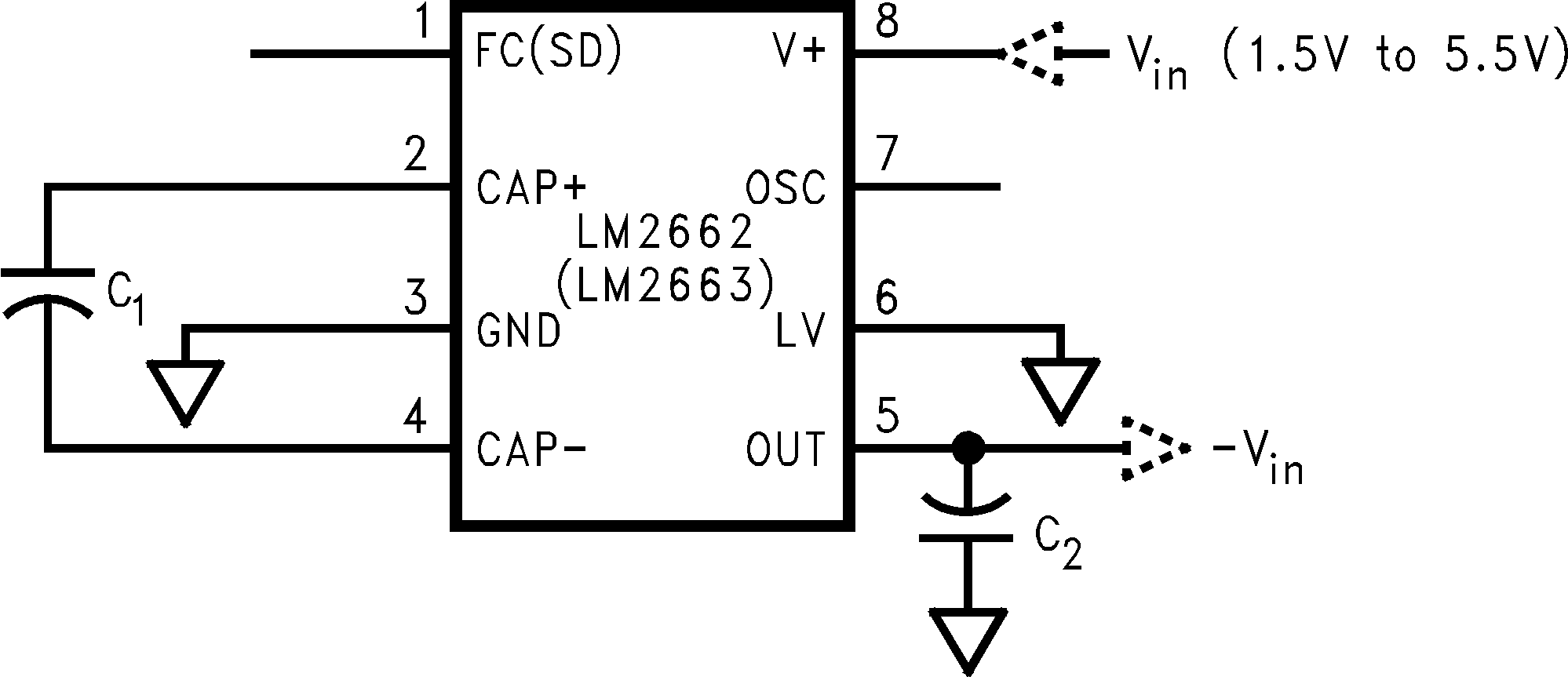 Figure 17. Simple Negative Voltage Converter
9.2.1.1 Design Requirements
The main application of LM2662/LM2663 is to generate a negative supply voltage. The voltage inverter circuit uses only two external capacitors as shown in Figure 17. The range of the input supply voltage is 1.5 V to 5.5 V. For a supply voltage less than 3.5 V, the LV pin must be connected to ground to bypass the internal regulator circuitry. This gives the best performance in low voltage applications. If the supply voltage is greater than 3.5 V, LV may be connected to ground or left open. The choice of leaving LV open simplifies the direct substitution of the LM2662/LM2663 for the LMC7660 Switched Capacitor Voltage Converter.
9.2.1.2 Detailed Design Procedure
The output characteristics of this circuit can be approximated by an ideal voltage source in series with a resistor. The voltage source equals −(V+). The output resistance Rout is a function of the ON resistance of the internal MOS switches, the oscillator frequency, and the capacitance and ESR of C1 and C2. Since the switching current charging and discharging C1 is approximately twice as the output current, the effect of the ESR of the pumping capacitor C1 is multiplied by four in the output resistance. The output capacitor C2 is charging and discharging at a current approximately equal to the output current, therefore, its ESR only counts once in the output resistance. A good approximation is:
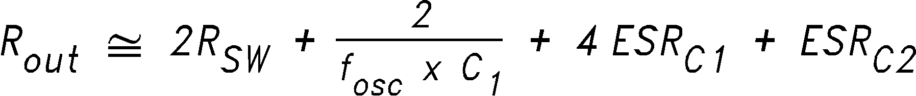
where RSW is the sum of the ON resistance of the internal MOS switches shown in the Voltage Inverting Principle.
High value, low ESR capacitors will reduce the output resistance. Instead of increasing the capacitance, the oscillator frequency can be increased to reduce the 2/(fosc × C1) term. Once this term is trivial compared with RSW and ESRs, further increasing in oscillator frequency and capacitance will become ineffective.
The peak-to-peak output voltage ripple is determined by the oscillator frequency, and the capacitance and ESR of the output capacitor C2:
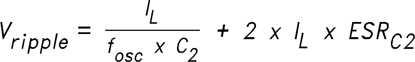
Again, using a low ESR capacitor will result in lower ripple.
9.2.1.2.1 Paralleling Devices
Any number of LM2662 devicess (or LM2663 devices) can be paralleled to reduce the output resistance. Each device must have its own pumping capacitor C1, while only one output capacitor Cout is needed as shown in Figure 18. The composite output resistance is:
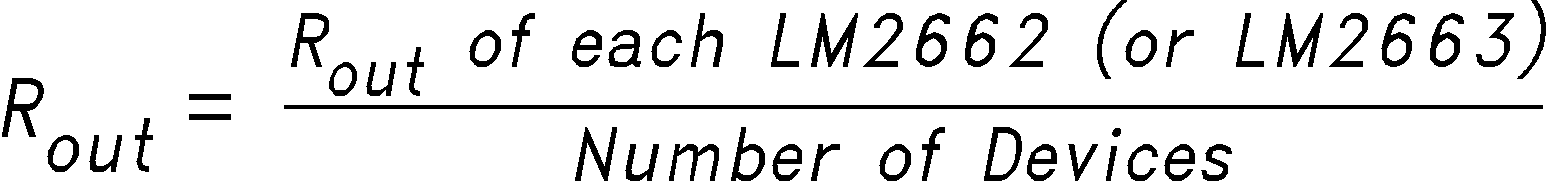
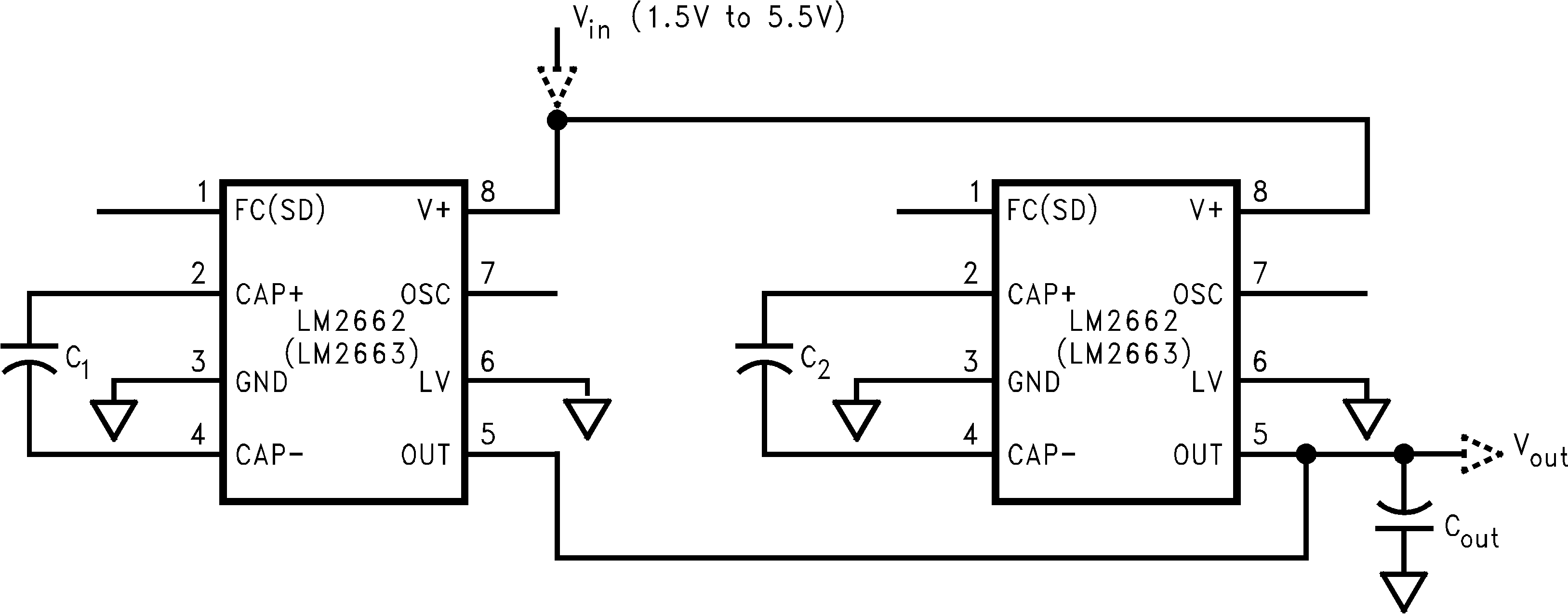 Figure 18. Lowering Output Resistance by Paralleling Devices
9.2.1.2.2 Cascading Devices
Cascading the LM2662 devices (or LM2663 devices) is an easy way to produce a greater negative voltage (as shown in Figure 19). If n is the integer representing the number of devices cascaded, the unloaded output voltage Vout is (−nVin). The effective output resistance is equal to the weighted sum of each individual device:

A three-stage cascade circuit shown in Figure 20 generates −3 Vin, from Vin.
Cascading is also possible when devices are operating in doubling mode. In Figure 21, two devices are cascaded to generate 3 Vin.
An example of using the circuit in Figure 20 or Figure 21 is generating +15 V or −15 V from a +5-V input.
Note that, the number of n is practically limited since the increasing of n significantly reduces the efficiency and increases the output resistance and output voltage ripple.
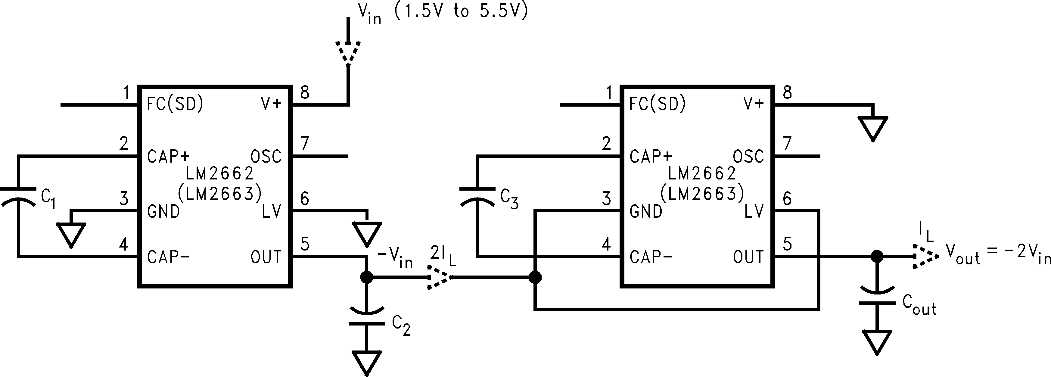 Figure 19. Increasing Output Voltage by Cascading Devices
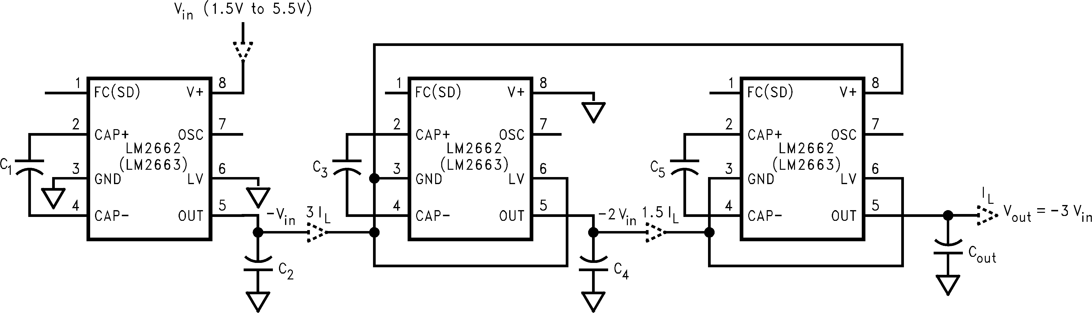 Figure 20. Generating −3 VIN From +VIN
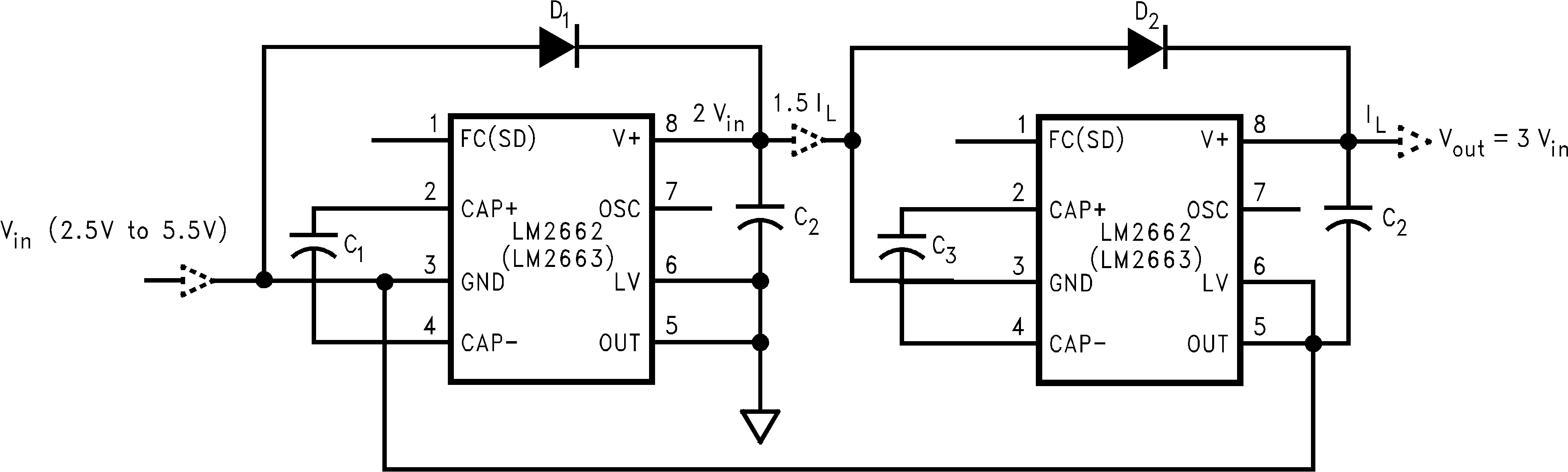 Figure 21. Generating +3 VIN From +VIN
9.2.1.2.3 Regulating VOUT
It is possible to regulate the output of the LM2662/LM2663 by use of a low dropout regulator (such as LP2986). The whole converter is depicted in Figure 22. This converter can give a regulated output from −1.5 V to −5.5 V by choosing the proper resistor ratio:
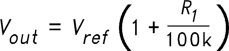
where
- Vref = 1.23V
The error flag on pin 7 of the LP2986 goes low when the regulated output at pin 5 drops by about 5% below nominal. The LP2986 can be shutdown by taking pin 8 low. The less than 1 μA quiescent current in the shutdown mode is favorable for battery powered applications.
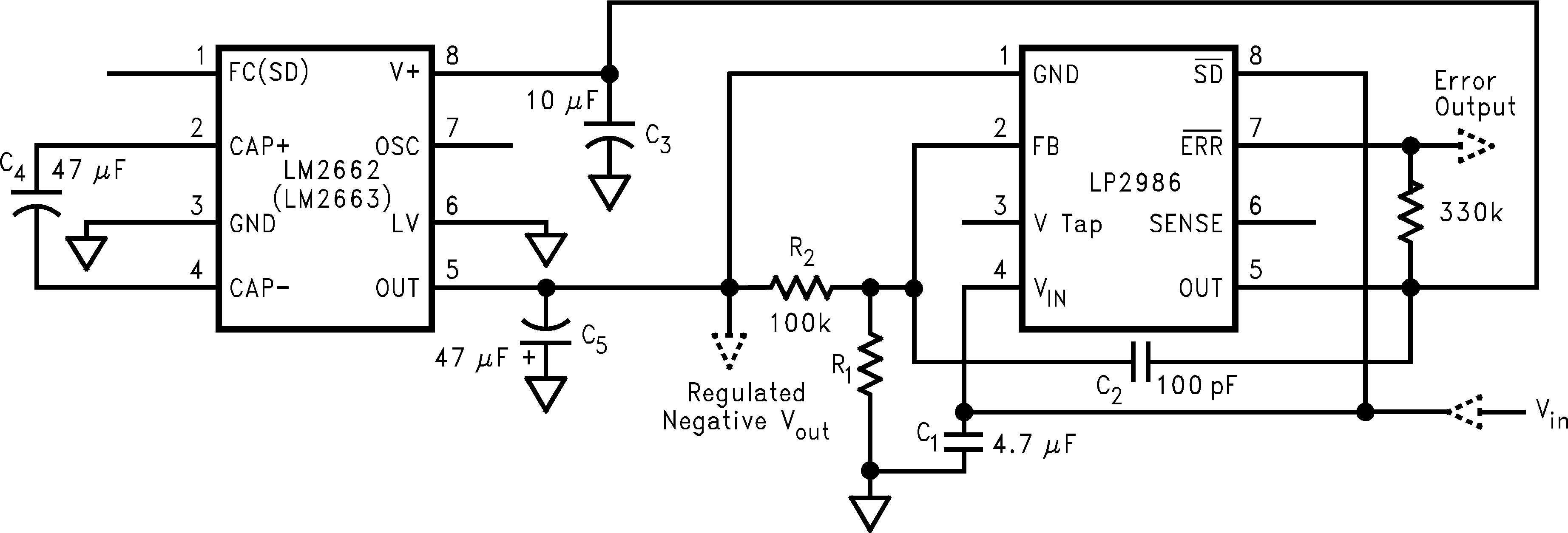 Figure 22. Combining LM2662/LM2663 With LP2986 to Make a Negative Adjustable Regulator
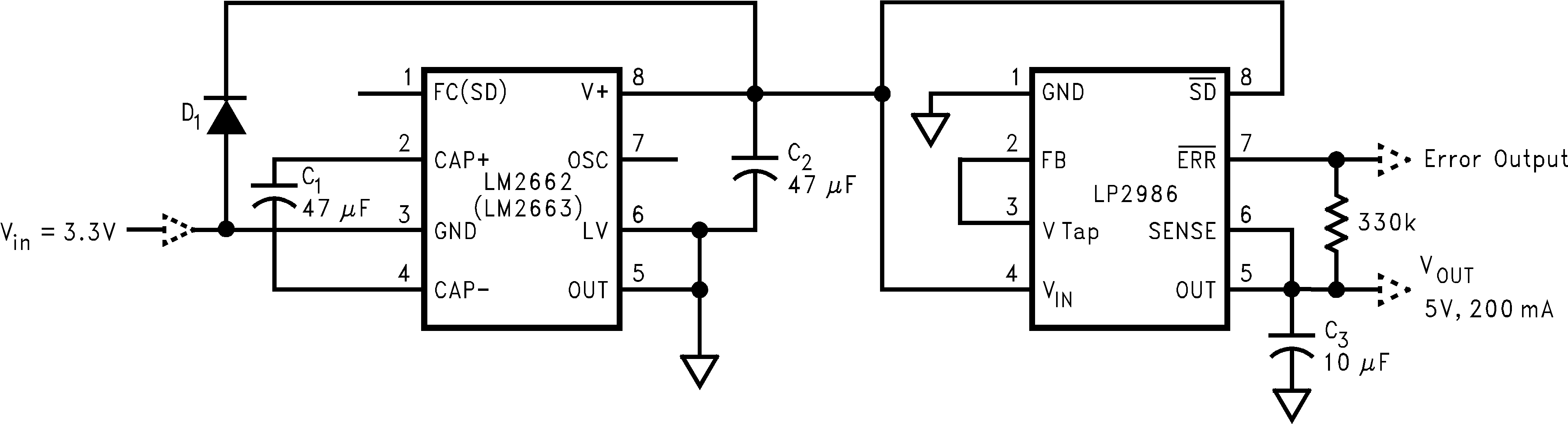
Also, as shown in Figure 23 by operating the LM2662/LM2663 in voltage doubling mode and adding a low dropout regulator (such as LP2986) at the output, we can get +5 V output from an input as low as +3.3 V.
9.2.1.3 Application Curves
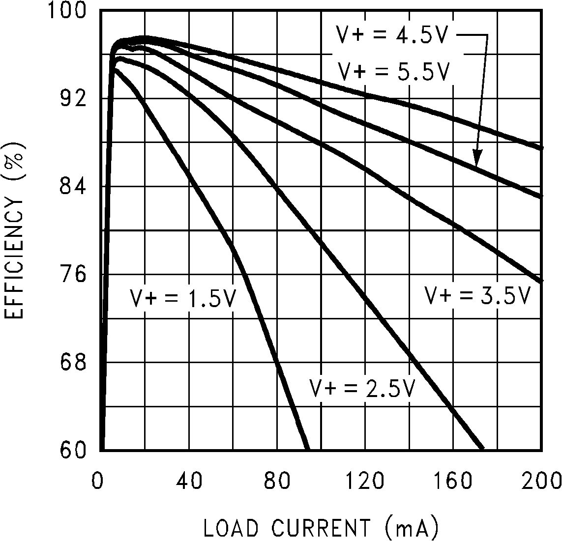 Figure 24. Efficiency vs Load Current
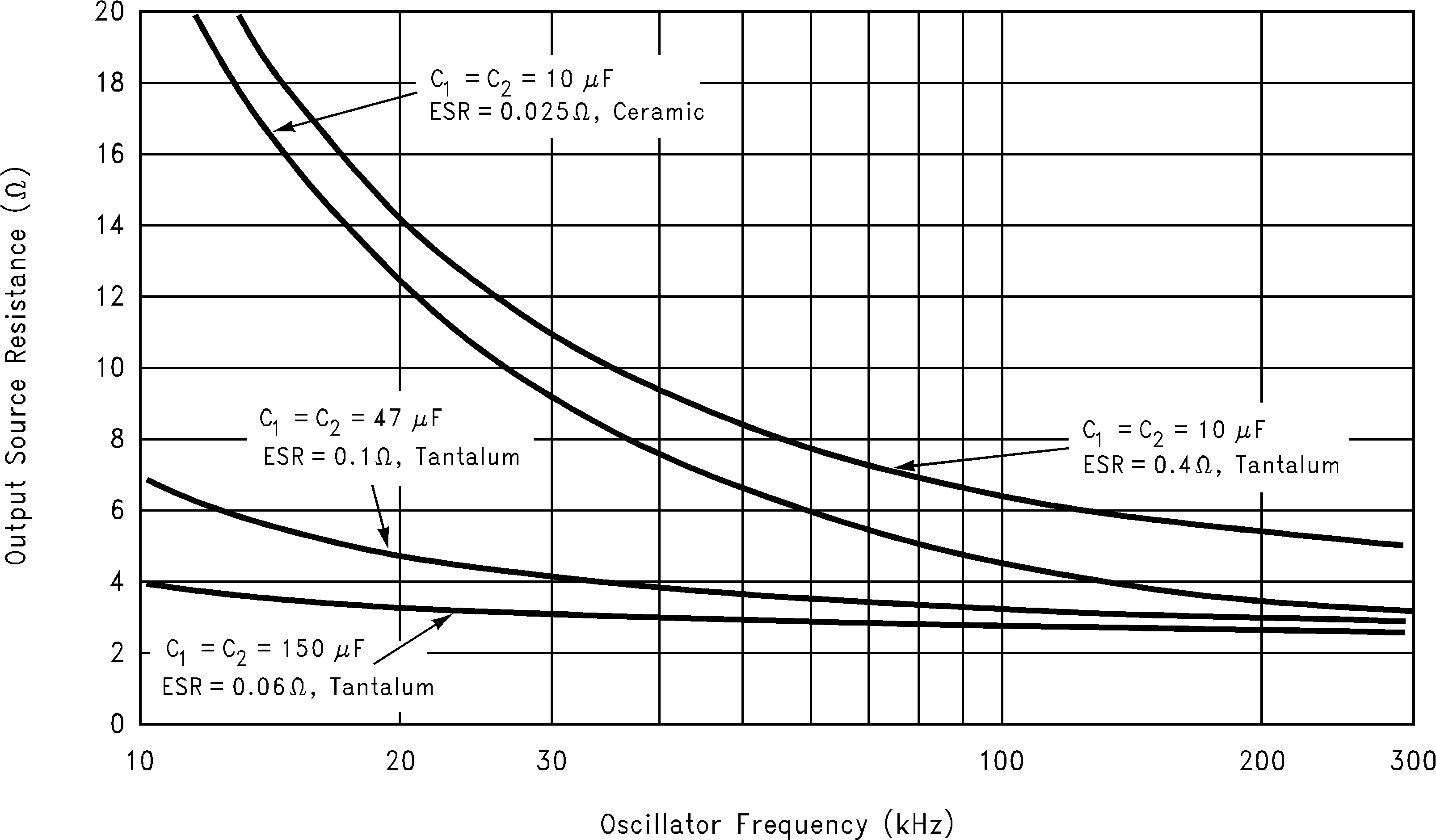 Figure 26. Output Source Resistance vs Oscillator Frequency
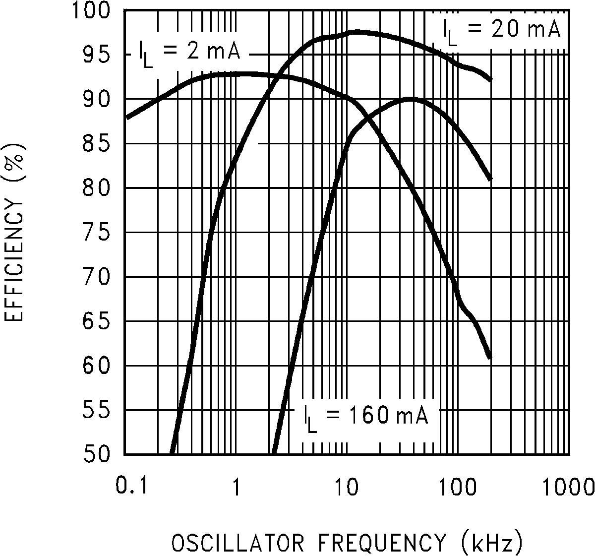 Figure 25. Efficiency vs Oscillator Frequency
9.2.2 Positive Voltage Doubler
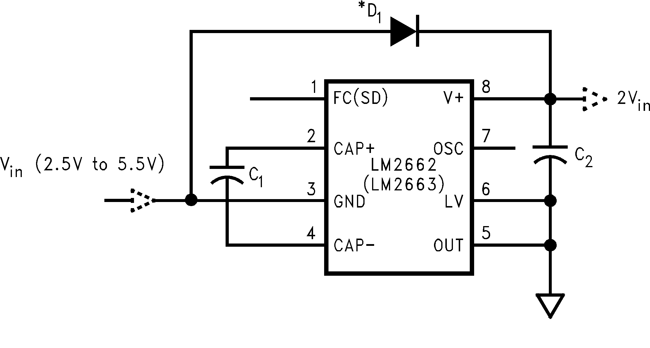 Figure 27. Positive Voltage Doubler
9.2.2.1 Design Requirements
The LM2662/LM2663 can operate as a positive voltage doubler (as shown in Figure 27). The doubling function is achieved by reversing some of the connections to the device.
9.2.2.2 Detailed Design Procedure
The input voltage is applied to the GND pin with an allowable voltage from 2.5 V to 5.5 V. The V+ pin is used as the output. The LV pin and OUT pin must be connected to ground. The OSC pin can not be driven by an external clock in this operation mode. The unloaded output voltage is twice of the input voltage and is not reduced by the diode D1's forward drop.
The Schottky diode D1 is only needed for start-up. The internal oscillator circuit uses the V+ pin and the LV pin (connected to ground in the voltage doubler circuit) as its power rails. Voltage across V+ and LV must be larger than 1.5 V to insure the operation of the oscillator. During start-up, D1 is used to charge up the voltage at V+ pin to start the oscillator; also, it protects the device from turning-on its own parasitic diode and potentially latching-up. Therefore, the Schottky diode D1 should have enough current carrying capability to charge the output capacitor at start-up, as well as a low forward voltage to prevent the internal parasitic diode from turning-on. A Schottky diode like 1N5817 can be used for most applications. If the input voltage ramp is less than 10 V/ms, a smaller Schottky diode like MBR0520LT1 can be used to reduce the circuit size.
9.2.2.3 Application Curves
See Application Curves section.
9.2.3 Splitting VIN in Half
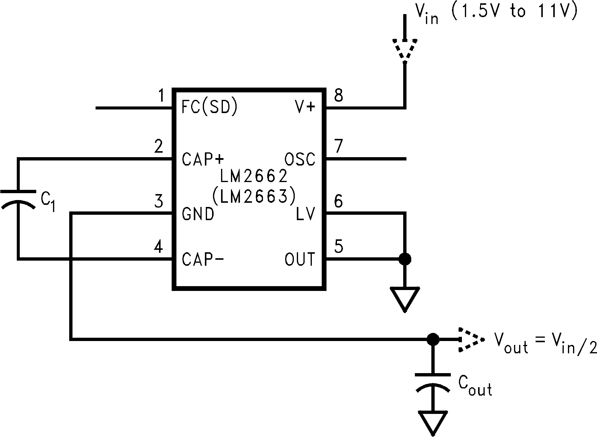 Figure 28. Splitting VIN in Half
9.2.3.1 Design Requirements
Another interesting application shown in Figure 28 is using the LM2662/LM2663 as a precision voltage divider. Since the off-voltage across each switch equals VIN/2, the input voltage can be raised to +11 V.
9.2.3.2 Detailed Design Procedure
As discussed in the Simple Negative Voltage Converter section, the output resistance and ripple voltage are dependent on the capacitance and ESR values of the external capacitors. The output voltage drop is the load current times the output resistance, and the power efficiency is
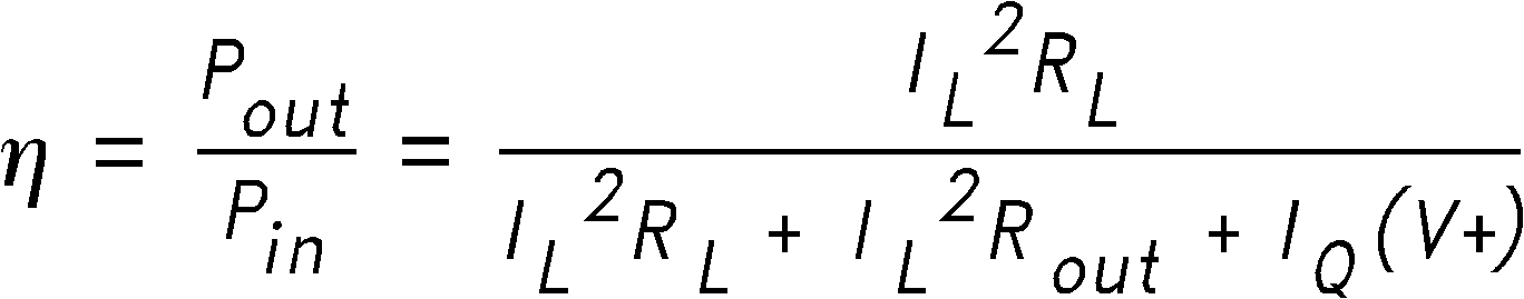
Where IQ(V+) is the quiescent power loss of the IC device, and IL2ROUT is the conversion loss associated with the switch on-resistance, the two external capacitors and their ESRs.
Low ESR capacitors are recommended for both capacitors to maximize efficiency, reduce the output voltage drop and voltage ripple. For convenience, C1 and C2 are usually chosen to be the same.
The output resistance varies with the oscillator frequency and the capacitors. In Figure 26, the output resistance vs. oscillator frequency curves are drawn for four difference capacitor values. At very low frequency range, capacitance plays the most important role in determining the output resistance. Once the frequency is increased to some point (such as 100 kHz for the 47-μF capacitors), the output resistance is dominated by the ON resistance of the internal switches and the ESRs of the external capacitors. A low value, smaller size capacitor usually has a higher ESR compared with a bigger size capacitor of the same type. Ceramic capacitors can be chosen for their lower ESR. As shown in Figure 26, in higher frequency range, the output resistance using the 10-μF ceramic capacitors is close to these using higher value tantalum capacitors.
9.2.3.3 Application Curves
See Application Curves section.