SNVS002E January 1999 – October 2014 LM2662 , LM2663
PRODUCTION DATA.
- 1 Features
- 2 Applications
- 3 Description
- 4 Revision History
- 5 Pin Configuration and Functions
- 6 Specifications
- 7 Parameter Measurement Information
- 8 Detailed Description
- 9 Application and Implementation
- 10Power Supply Recommendations
- 11Layout
- 12Device and Documentation Support
- 13Mechanical, Packaging, and Orderable Information
8 Detailed Description
8.1 Overview
The LM2662/LM2663 contains four large CMOS switches which are switched in a sequence to invert the input supply voltage. Energy transfer and storage are provided by external capacitors. Figure 16 illustrates the voltage conversion scheme. When S1 and S3 are closed, C1 charges to the supply voltage V+. During this time interval switches S2 and S4 are open. In the second time interval, S1 and S3 are open and S2 and S4 are closed, C1 is charging C2. After a number of cycles, the voltage across C2 will be pumped to V+. Since the anode of C2 is connected to ground, the output at the cathode of C2 equals −(V+) assuming no load on C2, no loss in the switches, and no ESR in the capacitors. In reality, the charge transfer efficiency depends on the switching frequency, the on-resistance of the switches, and the ESR of the capacitors.
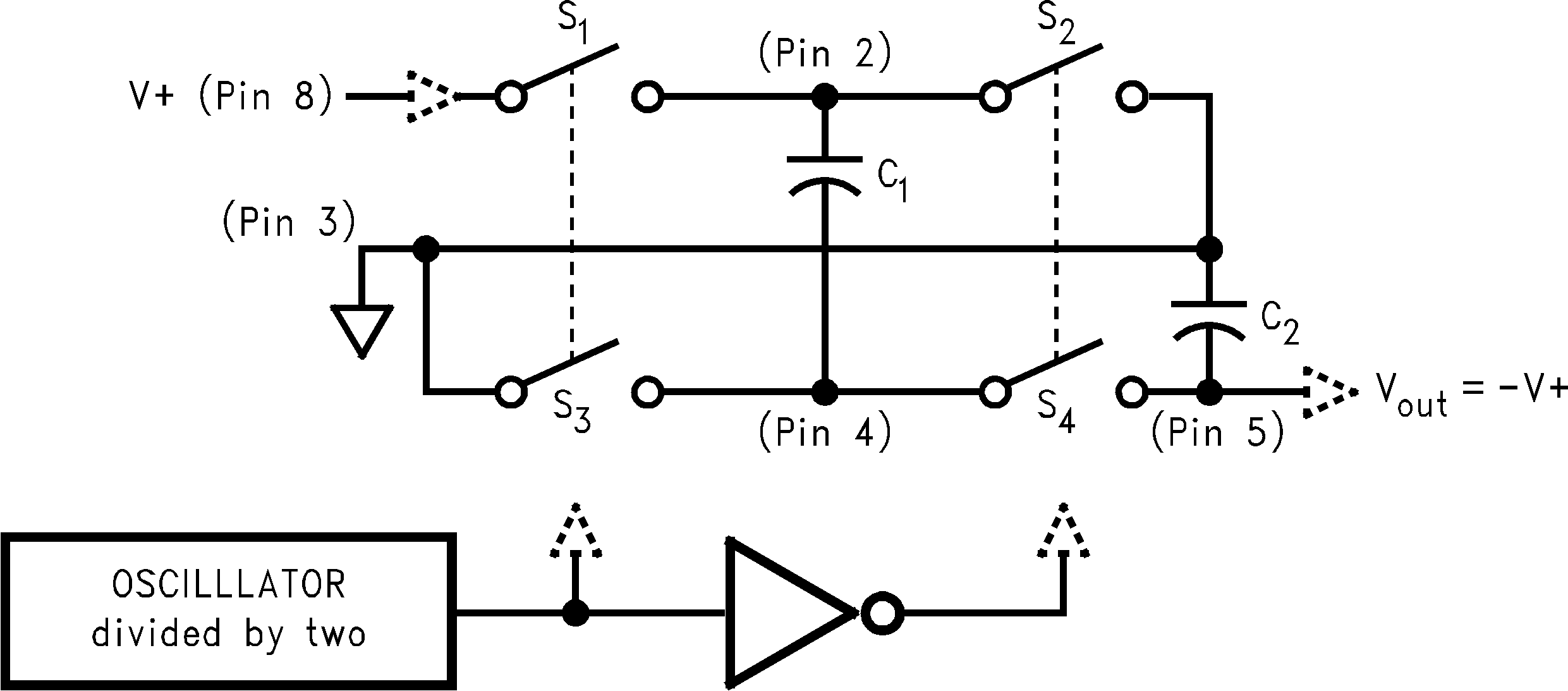 Figure 16. Voltage Inverting Principle
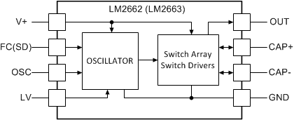
8.2 Functional Block Diagram
8.3 Feature Description
8.3.1 Changing Oscillator Frequency
For the LM2662, the internal oscillator frequency can be selected using the Frequency Control (FC) pin. When FC is open, the oscillator frequency is 20 kHz; when FC is connected to V+, the frequency increases to 150 kHz. A higher oscillator frequency allows smaller capacitors to be used for equivalent output resistance and ripple, but increases the typical supply current from 0.3 mA to 1.3 mA.
The oscillator frequency can be lowered by adding an external capacitor between OSC and GND (See typical performance characteristics). Also, in the inverter mode, an external clock that swings within 100 mV of V+ and GND can be used to drive OSC. Any CMOS logic gate is suitable for driving OSC. LV must be grounded when driving OSC. The maximum external clock frequency is limited to 150 kHz.
The switching frequency of the converter (also called the charge pump frequency) is half of the oscillator frequency.
NOTE
OSC cannot be driven by an external clock in the voltage-doubling mode.
Table 1. LM2662 Oscillator Frequency Selection
| FC | OSC | OSCILLATOR |
|---|---|---|
| Open | Open | 20 kHz |
| V+ | Open | 150 kHz |
| Open or V+ | External Capacitor | See Typical Performance Characteristics |
| N/A | External Clock (inverter mode only) | External Clock Frequency |
Table 2. LM2663 Oscillator Frequency Selection
| OSC | OSCILLATOR |
|---|---|
| Open | 150 kHz |
| External Capacitor | See Typical Performance Characteristics |
| External Clock (inverter mode only) | External Clock Frequency |
8.4 Device Functional Modes
8.4.1 Shutdown Mode
For the LM2663, a shutdown (SD) pin is available to disable the device and reduce the quiescent current to 10 μA. Applying a voltage greater than 2 V to the SD pin will bring the device into shutdown mode. While in normal operating mode, the SD pin is connected to ground.