ZHCS520E May   1996  – May 2019 LM2586

PRODUCTION DATA.  

  1. 特性
  2. 典型 应用
  3. 说明
    1.     Device Images
      1.      方框图
  4. 修订历史记录
  5. Pin Configurations
  6. Specifications
    1. 6.1 Absolute Maximum Ratings
    2. 6.2 ESD Ratings
    3. 6.3 Recommended Operating Ratings
    4. 6.4 Thermal Information
    5. 6.5 Electrical Characteristics: 3.3 V
    6. 6.6 Electrical Characteristics: 5 V
    7. 6.7 Electrical Characteristics: 12 V
    8. 6.8 Electrical Characteristics: Adjustable
    9. 6.9 Typical Characteristics
  7. Detailed Description
    1. 7.1 Overview
    2. 7.2 Functional Block Diagram
    3. 7.3 Feature Description
      1. 7.3.1 Flyback Regulator Operation
      2. 7.3.2 Step-Up (Boost) Regulator Operation
      3. 7.3.3 Programming Output Voltage (Selecting R1 And R2)
      4. 7.3.4 Shutdown Control
      5. 7.3.5 Frequency Adjustment
      6. 7.3.6 Frequency Synchronization
  8. Application and Implementation
    1. 8.1 Application Information
    2. 8.2 Typical Applications
      1. 8.2.1 Typical Flyback Regulator Applications
        1. 8.2.1.1 Design Requirements
          1. 8.2.1.1.1 Transformer Selection (T)
          2. 8.2.1.1.2 Transformer Footprints
        2. 8.2.1.2 Detailed Design Procedure
          1. 8.2.1.2.1 Custom Design With WEBENCH® Tools
          2. 8.2.1.2.2 Flyback Regulator Input Capacitors
          3. 8.2.1.2.3 Switch Voltage Limits
          4. 8.2.1.2.4 Output Voltage Limitations
          5. 8.2.1.2.5 Noisy Input Line Condition
          6. 8.2.1.2.6 Stability
      2. 8.2.2 Typical Boost Regulator Applications
        1. 8.2.2.1 Design Requirements
        2. 8.2.2.2 Detailed Design Procedure
    3. 8.3 System Examples
      1. 8.3.1 Test Circuits
  9. Layout
    1. 9.1 Layout Guidelines
    2. 9.2 Layout Example
  10. 10Heat Sink/Thermal Considerations
  11. 11器件和文档支持
    1. 11.1 器件支持
      1. 11.1.1 第三方产品免责声明
      2. 11.1.2 开发支持
        1. 11.1.2.1 使用 WEBENCH® 工具创建定制设计
    2. 11.2 接收文档更新通知
    3. 11.3 社区资源
    4. 11.4 商标
    5. 11.5 静电放电警告
    6. 11.6 Glossary
  12. 12机械、封装和可订购信息

封装选项

机械数据 (封装 | 引脚)
散热焊盘机械数据 (封装 | 引脚)
订购信息

Frequency Synchronization

Another feature of the LM2586 is the ability to synchronize the switching frequency to an external source, using the sync pin (pin 6). This feature allows the user to parallel multiple devices to deliver more output power.

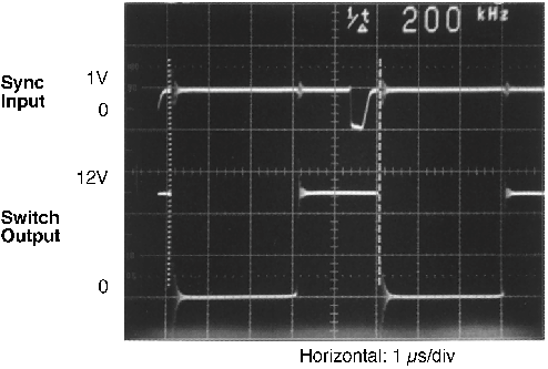
A negative falling pulse applied to the sync pin will synchronize the LM2586 to an external oscillator (see Figure 24 and Figure 25).

Use of this feature enables the LM2586 to be synchronized to an external oscillator, such as a system clock. This operation allows multiple power supplies to operate at the same frequency, thus eliminating frequency-related noise problems.

LM2586 01251659.pngFigure 24. Frequency Synchronization
LM2586 01251669.pngFigure 25. Waveforms of a Synchronized 12-V Boost Regulator

The scope photo in Figure 25 shows a LM2586 12-V boost regulator synchronized to a 200-kHz signal. There is a 700-ns delay between the falling edge of the sync signal and the turning on of the switch.
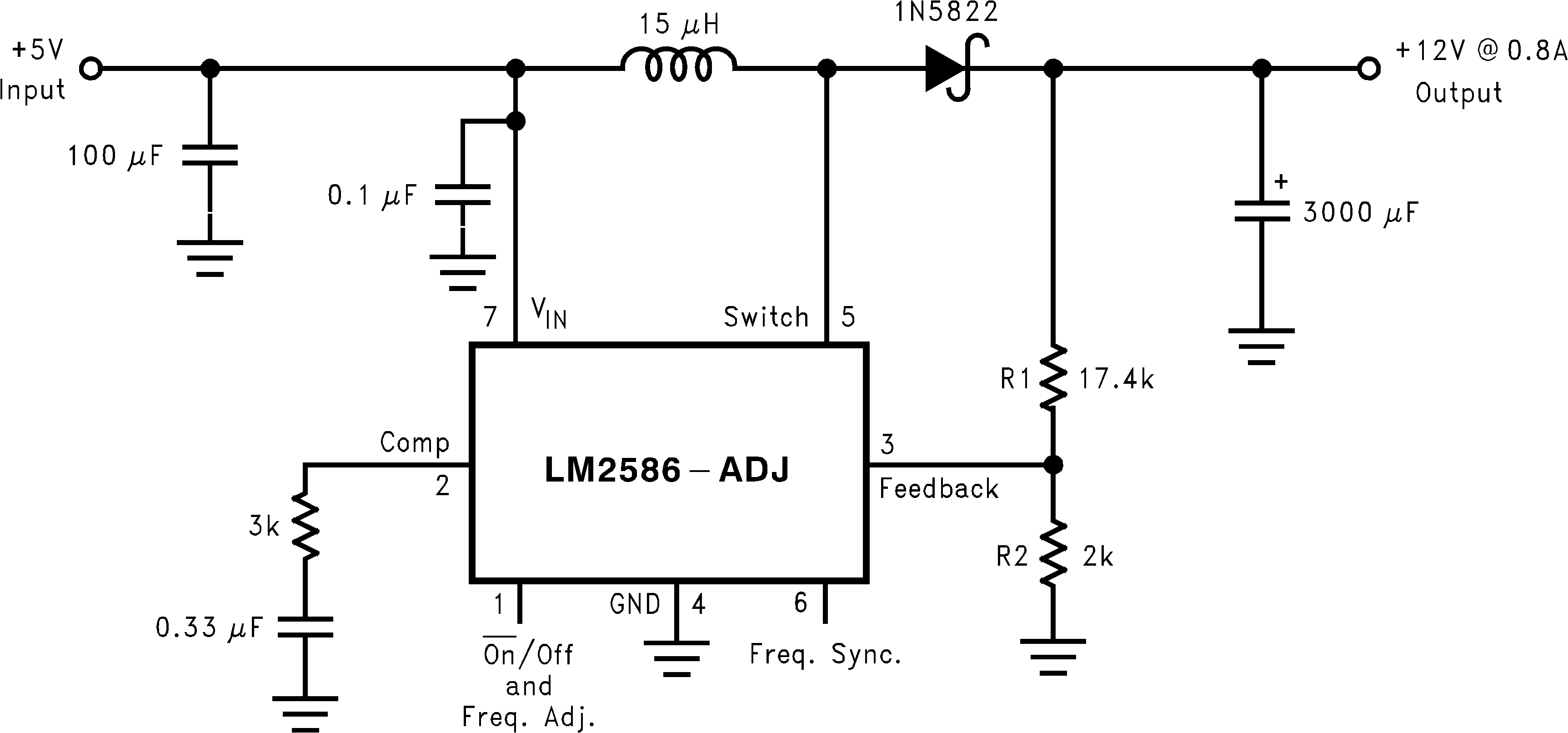
LM2586 01251661.pngFigure 26. Boost Regulator