ZHCSIJ1E June   1999  – July 2018 LM2574 , LM2574HV

PRODUCTION DATA.  

  1. 特性
  2. 应用
  3. 说明
    1.     Device Images
      1.      典型应用(固定输出电压版本)
  4. 修订历史记录
  5. Pin Configuration and Functions
    1.     Pin Functions
  6. Specifications
    1. 6.1  Absolute Maximum Ratings
    2. 6.2  ESD Ratings
    3. 6.3  Recommended Operating Conditions
    4. 6.4  Thermal Information
    5. 6.5  Electrical Characteristics for All Output Voltage Versions
    6. 6.6  Electrical Characteristics – 3.3-V Version
    7. 6.7  Electrical Characteristics – 5-V Version
    8. 6.8  Electrical Characteristics – 12-V Version
    9. 6.9  Electrical Characteristics – 15-V Version
    10. 6.10 Electrical Characteristics – Adjustable Version
    11. 6.11 Typical Characteristics
  7. Detailed Description
    1. 7.1 Overview
    2. 7.2 Functional Block Diagram
    3. 7.3 Feature Description
      1. 7.3.1 Current Limit
      2. 7.3.2 Undervoltage Lockout
      3. 7.3.3 Delayed Start-Up
      4. 7.3.4 Adjustable Output, Low-Ripple Power Supply
    4. 7.4 Device Functional Modes
      1. 7.4.1 Shutdown Mode
      2. 7.4.2 Active Mode
  8. Application and Implementation
    1. 8.1 Application Information
      1. 8.1.1 Input Capacitor (CIN)
      2. 8.1.2 Inductor Selection
      3. 8.1.3 Inductor Ripple Current
      4. 8.1.4 Output Capacitor
      5. 8.1.5 Catch Diode
      6. 8.1.6 Output Voltage Ripple and Transients
      7. 8.1.7 Feedback Connection
      8. 8.1.8 ON/OFF Input
      9. 8.1.9 Additional Applications
        1. 8.1.9.1 Inverting Regulator
        2. 8.1.9.2 Negative Boost Regulator
    2. 8.2 Typical Applications
      1. 8.2.1 Fixed Output Voltage Applications
        1. 8.2.1.1 Design Requirements
        2. 8.2.1.2 Detailed Design Procedure
          1. 8.2.1.2.1 Custom Design With WEBENCH® Tools
          2. 8.2.1.2.2 Inductor Selection (L1)
          3. 8.2.1.2.3 Output Capacitor Selection (COUT)
          4. 8.2.1.2.4 Catch Diode Selection (D1)
          5. 8.2.1.2.5 Input Capacitor (CIN)
        3. 8.2.1.3 Application Curves
      2. 8.2.2 Adjustable Output Voltage Applications
        1. 8.2.2.1 Design Requirements
        2. 8.2.2.2 Detailed Design Procedure
          1. 8.2.2.2.1 Programming Output Voltage
          2. 8.2.2.2.2 Inductor Selection (L1)
          3. 8.2.2.2.3 Output Capacitor Selection (COUT)
          4. 8.2.2.2.4 Catch Diode Selection (D1)
          5. 8.2.2.2.5 Input Capacitor (CIN)
        3. 8.2.2.3 Application Curves
  9. Power Supply Recommendations
  10. 10Layout
    1. 10.1 Layout Guidelines
    2. 10.2 Layout Example
    3. 10.3 Grounding
    4. 10.4 Thermal Considerations
  11. 11器件和文档支持
    1. 11.1 器件支持
      1. 11.1.1 第三方产品免责声明
      2. 11.1.2 使用 WEBENCH® 工具创建定制设计
      3. 11.1.3 器件命名规则
        1. 11.1.3.1  降压稳压器
        2. 11.1.3.2  降压/升压稳压器
        3. 11.1.3.3  占空比 (D)
        4. 11.1.3.4  环流二极管或导流二极管
        5. 11.1.3.5  电容器等效串联电阻 (ESR)
        6. 11.1.3.6  等效串联电感 (ESL)
        7. 11.1.3.7  输出纹波电压
        8. 11.1.3.8  电容器纹波电流
        9. 11.1.3.9  待机静态电流 (ISTBY)
        10. 11.1.3.10 电感器纹波电流 (ΔiIND)
        11. 11.1.3.11 连续与非连续模式运行
        12. 11.1.3.12 电感器饱和
        13. 11.1.3.13 运算伏特微秒常数 (E × Top)
    2. 11.2 文档支持
      1. 11.2.1 相关文档
    3. 11.3 接收文档更新通知
    4. 11.4 社区资源
    5. 11.5 商标
    6. 11.6 静电放电警告
    7. 11.7 术语表
  12. 12机械、封装和可订购信息

封装选项

机械数据 (封装 | 引脚)
散热焊盘机械数据 (封装 | 引脚)
订购信息

Typical Characteristics

See Figure 27.
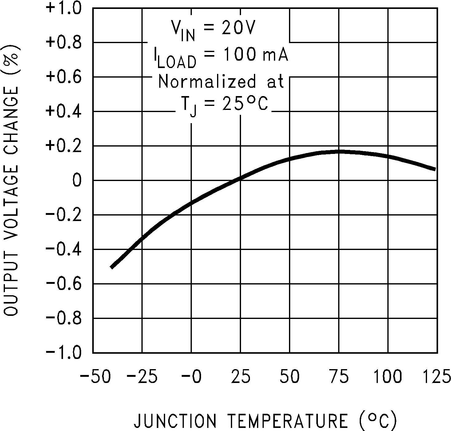
LM2574 LM2574HV 01139427.png
Figure 1. Normalized Output Voltage
LM2574 LM2574HV 01139429.png
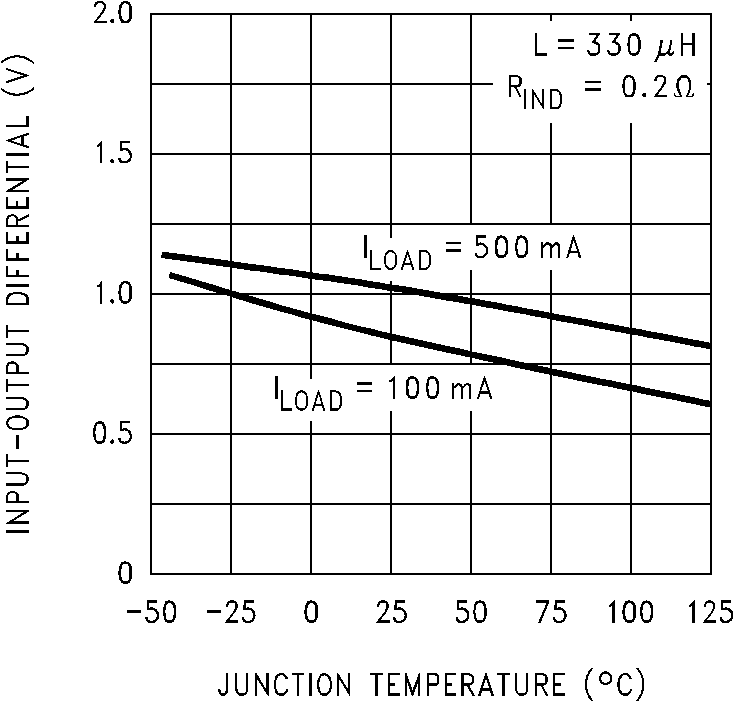
Figure 3. Dropout Voltage
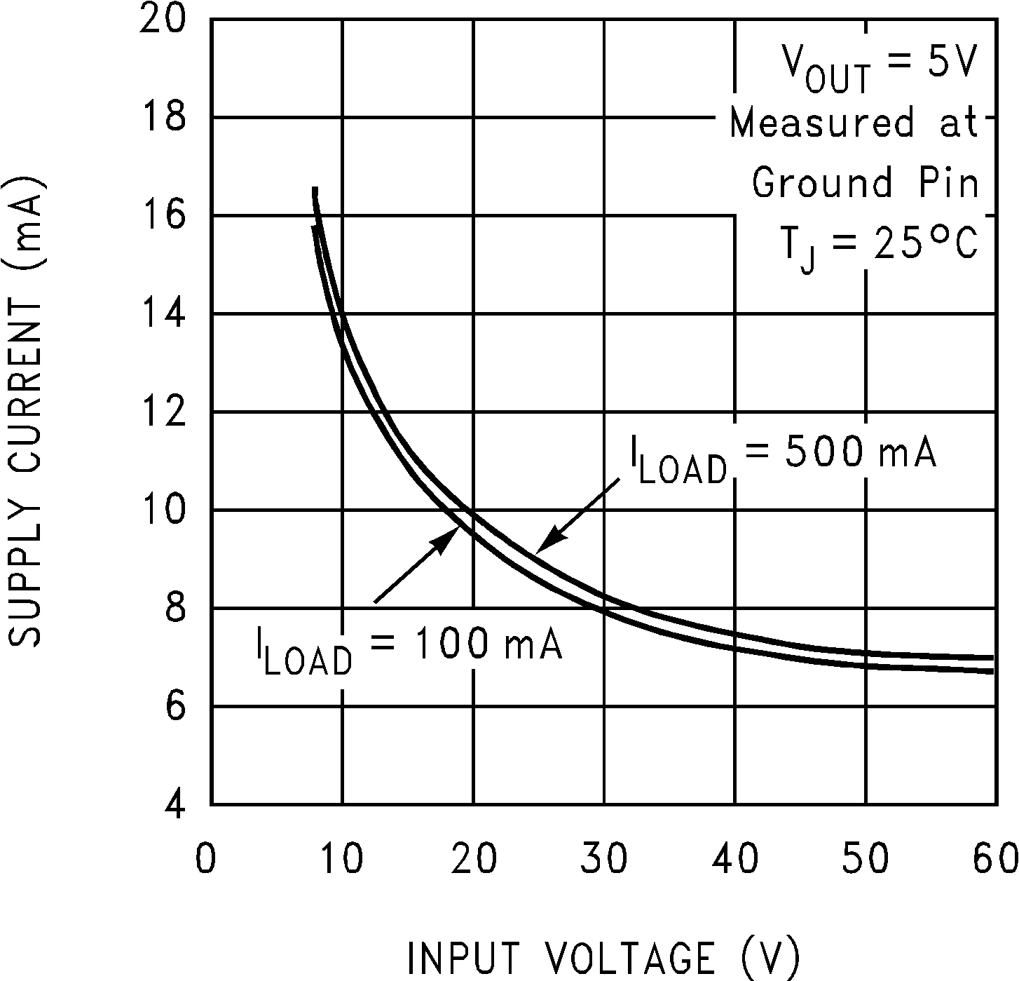
LM2574 LM2574HV 01139431.png
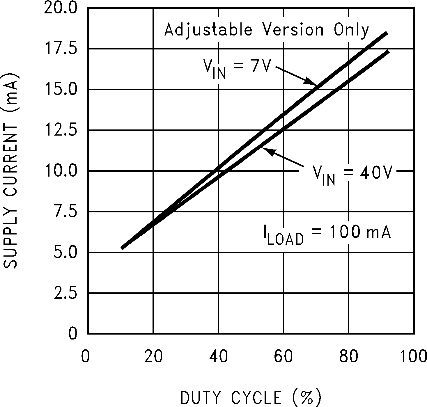
Figure 5. Supply Current
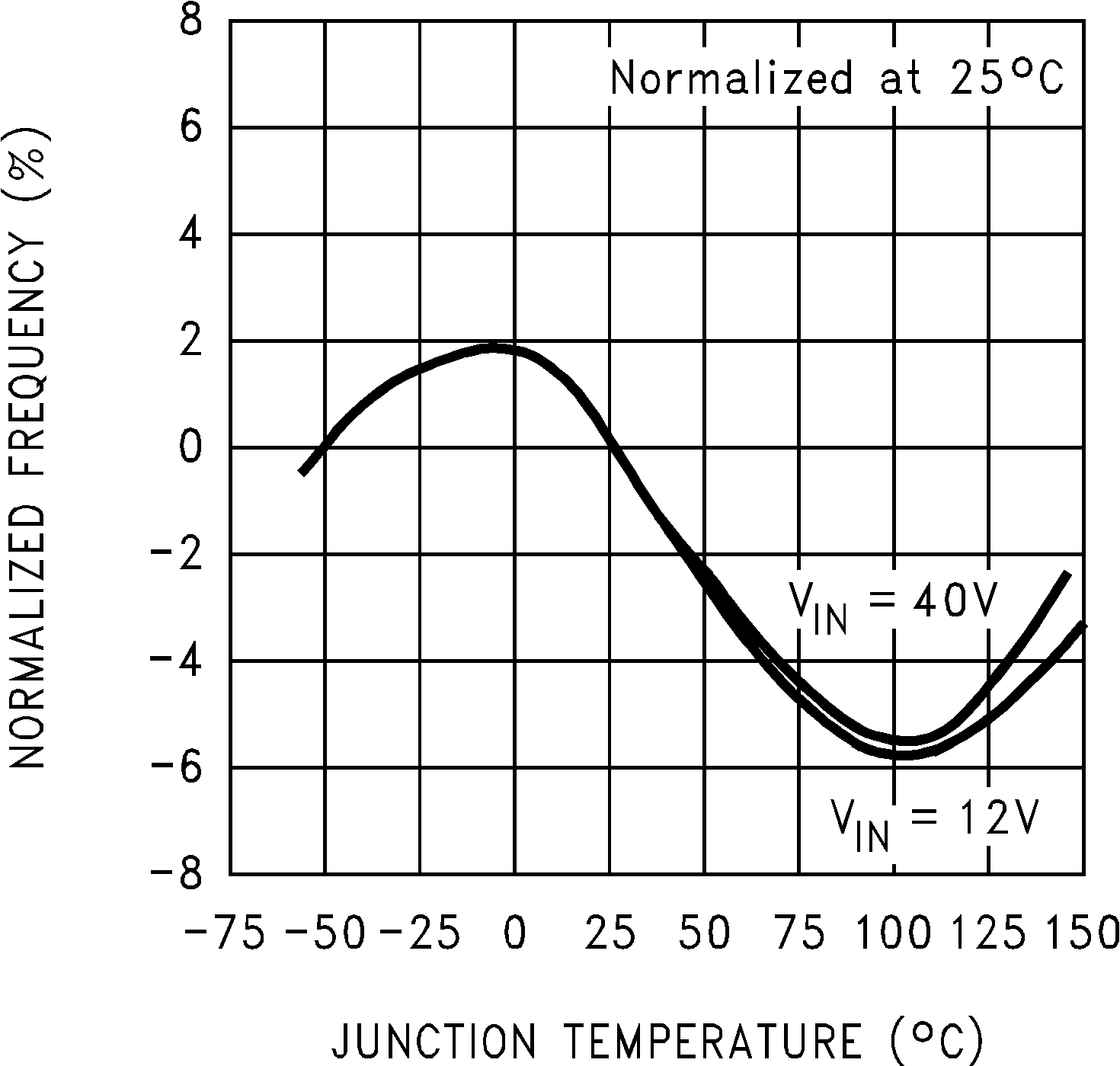
LM2574 LM2574HV 01139433.png
Figure 7. Oscillator Frequency
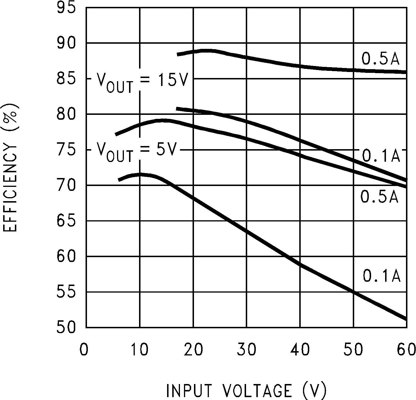
LM2574 LM2574HV 01139435.png
Figure 9. Efficiency
LM2574 LM2574HV 01139437.png
Figure 11. Supply Current vs Duty Cycle
LM2574 LM2574HV 01139439.png
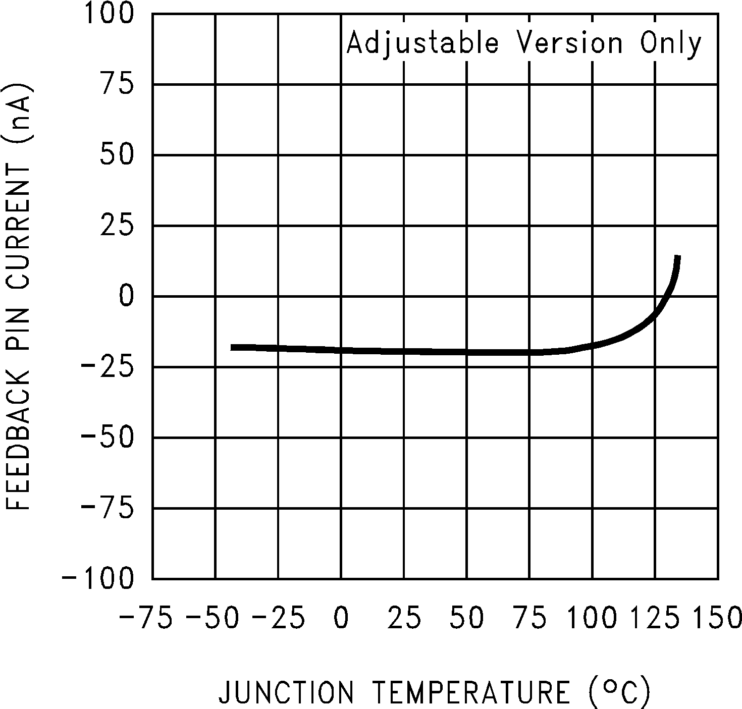
Figure 13. Feedback Pin Current
LM2574 LM2574HV 01139428.png
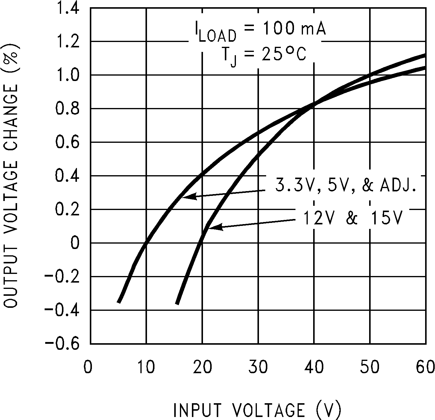
Figure 2. Line Regulation
LM2574 LM2574HV 01139430.png
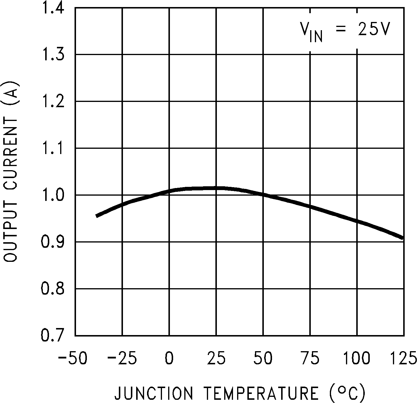
Figure 4. Current Limit
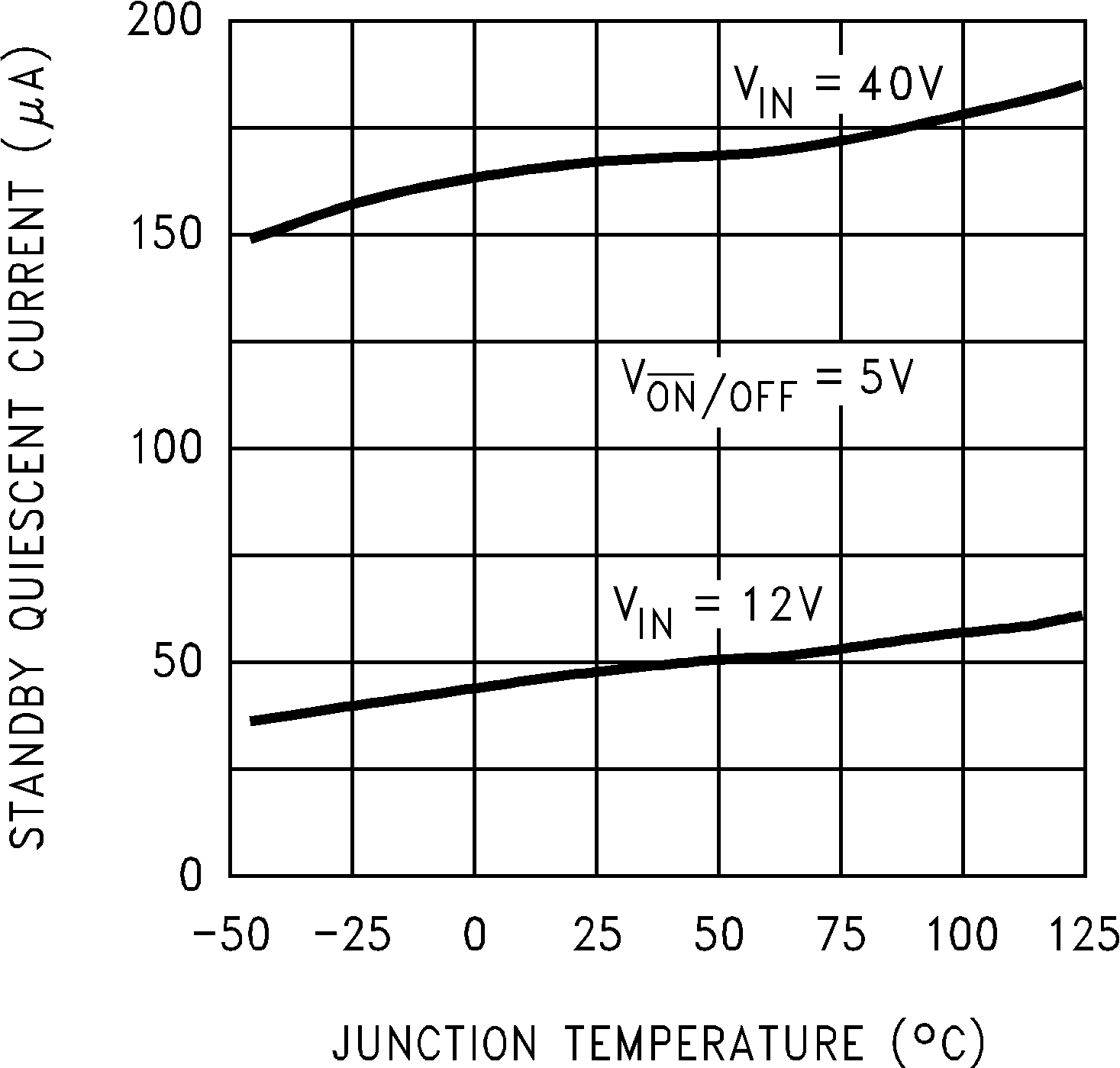
LM2574 LM2574HV 01139432.png
Figure 6. Standby Quiescent Current
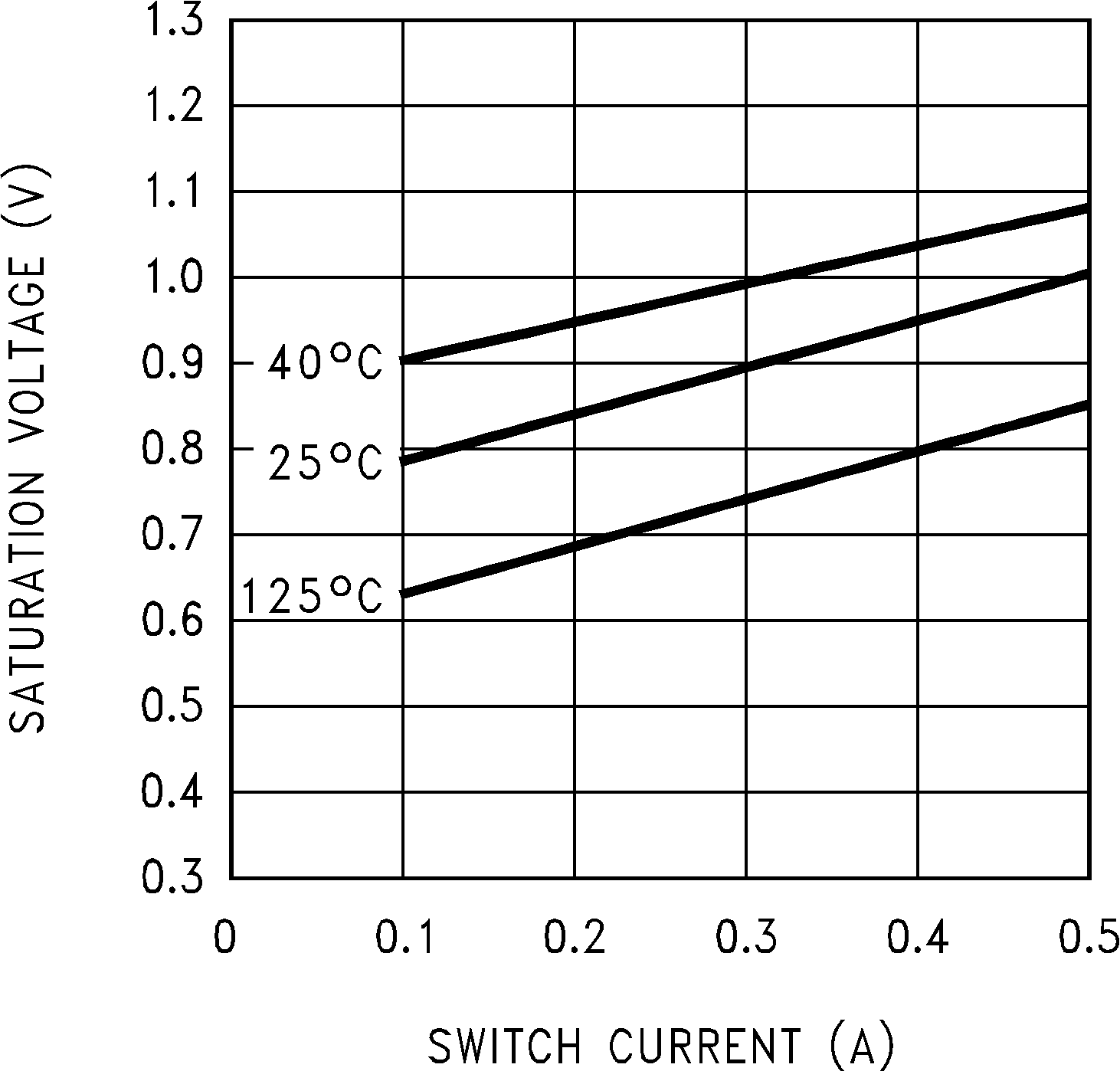
LM2574 LM2574HV 01139434.png
Figure 8. Switch Saturation Voltage
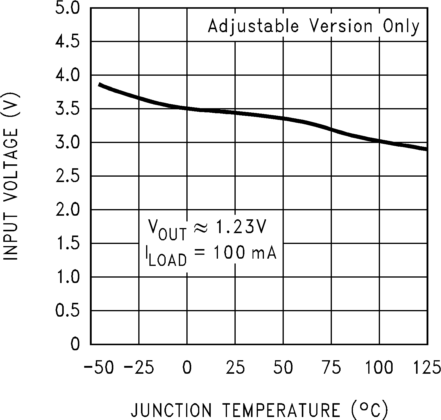
LM2574 LM2574HV 01139436.png
Figure 10. Minimum Operating Voltage
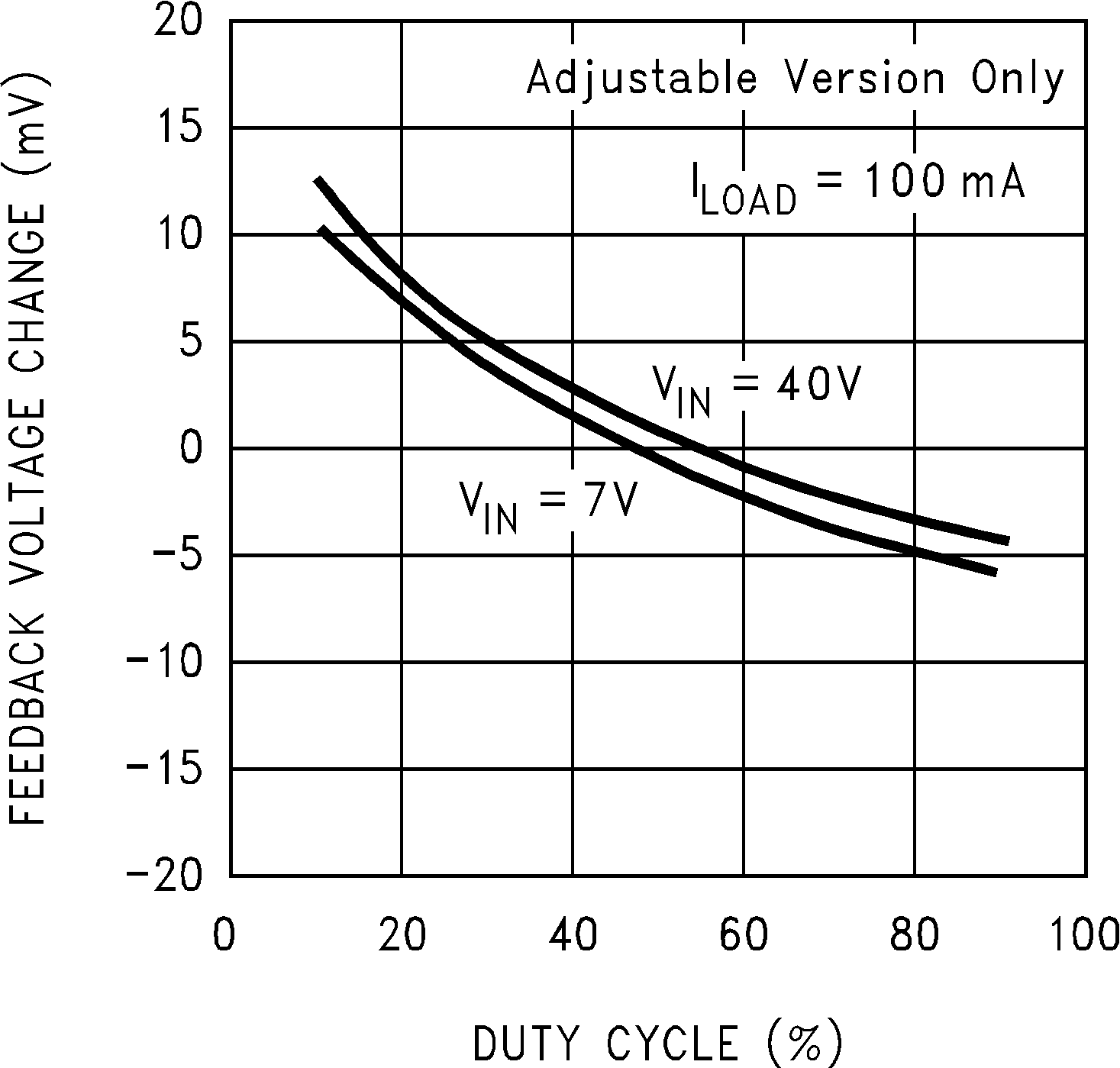
LM2574 LM2574HV 01139438.png
Figure 12. Feedback Voltage vs Duty Cycle
LM2574 LM2574HV 01139440.png
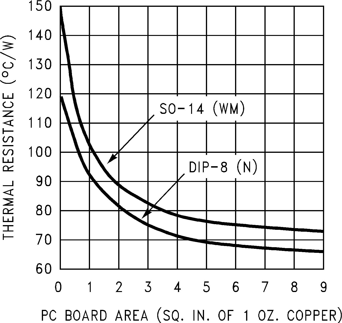
Figure 14. Junction-to-Ambient Thermal Resistance