SNVS639G December 2009 – December 2015 LM21305
PRODUCTION DATA.
- 1 Features
- 2 Applications
- 3 Description
- 4 Revision History
- 5 Description (continued)
- 6 Pin Configuration and Functions
- 7 Specifications
-
8 Detailed Description
- 8.1 Overview
- 8.2 Functional Block Diagram
- 8.3
Feature Description
- 8.3.1 Synchronous DC-DC Switching Converter
- 8.3.2 Peak Current-Mode Control
- 8.3.3 Switching Frequency Setting and Synchronization
- 8.3.4 Light-Load Operation
- 8.3.5 Precision Enable
- 8.3.6 Device Enable, Soft-Start, and Pre-Bias Startup Capability
- 8.3.7 Peak Current Protection and Negative Current Limiting
- 8.3.8 PGOOD Indicator
- 8.3.9 Internal Bias Regulators
- 8.3.10 Minimum On-Time Considerations
- 8.4 Device Functional Modes
-
9 Application and Implementation
- 9.1 Application Information
- 9.2
Typical Application
- 9.2.1 Design Requirements
- 9.2.2
Detailed Design Procedure
- 9.2.2.1 Setting the Output Voltage
- 9.2.2.2 Calculating the Duty Cycle
- 9.2.2.3 Input Capacitors
- 9.2.2.4 AVIN Filter
- 9.2.2.5 Switching Frequency Selection
- 9.2.2.6 Filter Inductor
- 9.2.2.7 Output Capacitor
- 9.2.2.8 Efficiency Considerations
- 9.2.2.9 Load Current Derating When Duty Cycle Exceeds 50%
- 9.2.2.10 Control Loop Compensation
- 9.2.2.11 Compensation Components Selection
- 9.2.2.12 Plotting the Loop Gain
- 9.2.2.13 High Frequency Considerations
- 9.2.2.14 Bootstrap Capacitor
- 9.2.2.15 5V0 and 2V5 Capacitors
- 9.2.2.16 Maximum Ambient Temperature
- 9.2.3 Application Curves
- 10Power Supply Recommendations
- 11Layout
- 12Device and Documentation Support
- 13Mechanical, Packaging, and Orderable Information
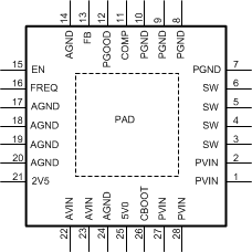
6 Pin Configuration and Functions
RSG Package
28-Pin WQFN with Exposed Thermal Pad
Top View

Pin Functions
| PIN | Type(1) | DESCRIPTION | |
|---|---|---|---|
| NAME | NO. | ||
| 2V5 | 21 | P | 2.5-V output of the internal LDO regulator. Bypass to AGND with a 0.1-µF ceramic capacitor. Loading this pin is not recommended. |
| 5V0 | 25 | P | 5.0-V output of the internal LDO regulator. Bypass to PGND with a 1-µF ceramic capacitor. Loading this pin is not recommended. |
| AGND | 14, 17–20, 24 | G | Analog ground for the internal bias circuitry and signal return connection for analog functions, including COMP network, frequency adjust resistor, and 2V5 decoupling capacitor. |
| AVIN | 22, 23 | P | Analog power input. AVIN powers the internal 2.5-V and 5.0-V LDOs that provide bias current and internal driver power, respectively. AVIN can be connected to PVIN through a low-pass RC filter or can be supplied by a separate rail. |
| CBOOT | 26 | P | High-side bootstrap connection to drive the high-side MOSFET. Connect a 100-nF bootstrap capacitor between the CBOOT and SW pins. |
| COMP | 11 | A | Compensation node. This pin is an output voltage control loop error amplifier output. Connect an external compensation network to ensure stability. |
| EN | 15 | I | Precision enable pin. Use an external divider to set the device turn-on threshold. If not used, connect the EN pin to AVIN. |
| FB | 13 | A | Voltage feedback pin. Connect this pin to the output voltage directly or through a resistor divider to set the output voltage range. |
| FREQ | 16 | A | Frequency adjust pin. Connect a resistor from FREQ to AGND to set the internal oscillator frequency. Connect FREQ to an external clock source via a coupling capacitor to synchronize to the external clock frequency. |
| PVIN | 1, 2, 27, 28 | P | Input voltage to the power MOSFETs inside the device. |
| SW | 3-6 | P | Switch node output of the power MOSFETs. Voltage swings from PVIN to GND on this pin. SW also delivers current to the external inductor. |
| PGND | 7–10 | G | Power ground connection for the internal power switches. |
| PGOOD | 12 | OD | Open-drain output with 16 μs of built-in deglitch time. If high, this status pin indicates that the output voltage is regulated within tolerance. Connect a 10-kΩ to 100-kΩ resistor to a pullup voltage source, for example the 5V0 rail or auxiliary system voltage rail. |
| PAD | PAD | — | Exposed pad at the back of the device. Connect PAD to PGND, but PAD cannot be used as the primary ground connection. Use multiple vias under PAD to connect to the system ground plane for optimal thermal performance. |
(1) P: Power, A: Analog, I: Digital Input, OD: Open Drain, G: Ground.