SNVS639G December 2009 – December 2015 LM21305
PRODUCTION DATA.
- 1 Features
- 2 Applications
- 3 Description
- 4 Revision History
- 5 Description (continued)
- 6 Pin Configuration and Functions
- 7 Specifications
-
8 Detailed Description
- 8.1 Overview
- 8.2 Functional Block Diagram
- 8.3
Feature Description
- 8.3.1 Synchronous DC-DC Switching Converter
- 8.3.2 Peak Current-Mode Control
- 8.3.3 Switching Frequency Setting and Synchronization
- 8.3.4 Light-Load Operation
- 8.3.5 Precision Enable
- 8.3.6 Device Enable, Soft-Start, and Pre-Bias Startup Capability
- 8.3.7 Peak Current Protection and Negative Current Limiting
- 8.3.8 PGOOD Indicator
- 8.3.9 Internal Bias Regulators
- 8.3.10 Minimum On-Time Considerations
- 8.4 Device Functional Modes
-
9 Application and Implementation
- 9.1 Application Information
- 9.2
Typical Application
- 9.2.1 Design Requirements
- 9.2.2
Detailed Design Procedure
- 9.2.2.1 Setting the Output Voltage
- 9.2.2.2 Calculating the Duty Cycle
- 9.2.2.3 Input Capacitors
- 9.2.2.4 AVIN Filter
- 9.2.2.5 Switching Frequency Selection
- 9.2.2.6 Filter Inductor
- 9.2.2.7 Output Capacitor
- 9.2.2.8 Efficiency Considerations
- 9.2.2.9 Load Current Derating When Duty Cycle Exceeds 50%
- 9.2.2.10 Control Loop Compensation
- 9.2.2.11 Compensation Components Selection
- 9.2.2.12 Plotting the Loop Gain
- 9.2.2.13 High Frequency Considerations
- 9.2.2.14 Bootstrap Capacitor
- 9.2.2.15 5V0 and 2V5 Capacitors
- 9.2.2.16 Maximum Ambient Temperature
- 9.2.3 Application Curves
- 10Power Supply Recommendations
- 11Layout
- 12Device and Documentation Support
- 13Mechanical, Packaging, and Orderable Information
1 Features
- High-Efficiency Synchronous DC-DC Converter:
- External Frequency Synchronization
- Accurate 0.598-V Feedback Voltage Reference
- Ultra-Fast Line and Load Transient Response:
- Peak Current-Mode Control
- Internal Slope Compensation
- High-Bandwidth Error Amplifier
- Ultra-Low Shutdown Quiescent Current
- Wide Duty-Cycle Operating Range:
- TON-MIN: 70 ns for Low VOUT
- TOFF-MIN: 50 ns for High Duty Cycle
- Diode Emulation Mode at Light Loads
- Integrated Bias Supply LDO Sub-Regulators
- Internal Soft-Start Function:
- Monotonic Startup into Pre-Biased Loads
- Precision Enable Input with Hysteresis
- Open-Drain PGOOD Indicator
- Internal Input Undervoltage Lockout (UVLO)
- Cycle-by-Cycle Overcurrent Protection
- Output Overvoltage Protection (OVP)
- Thermal Shutdown Protection with Hysteresis
- 5-mm x 5-mm WQFN-28 PowerPAD™ Package
2 Applications
- DC-DC Converters and POL Modules
- DSP and FPGA Core Voltage Supplies
- Telecommunications Infrastructure
- Embedded Computing, Servers, and Storage
3 Description
The LM21305 is a full-featured, 5-A, synchronous buck dc-dc converter optimized for solution size, flexibility, and high conversion efficiency. High-power density LM21305 designs are easily achieved by virtue of monolithic integration of high-side and low-side power MOSFETs, high switching frequency, peak current-mode control, and optimized thermal design. The efficiency of the LM21305 is maximized at light loads with diode emulation mode operation and at heavy loads by optimal design of the MOSFET adaptive gate drivers to minimize switch dead-times and body-diode conduction losses.
The LM21305 accepts a wide input voltage range of 3 V to 18 V for interface to various intermediate bus voltages, including 3.3-V, 5-V, and 12-V rails. A 1.5% voltage reference and 70-ns, high-side MOSFET minimum controllable on-time enable output voltages as low as 0.598 V with excellent setpoint accuracy. The LM21305 is available in a 5-mm × 5-mm2 WQFN-28 thermally-enhanced package with 0.5-mm pitch.
Device Information(1)
| PART NUMBER | PACKAGE | BODY SIZE (NOM) |
|---|---|---|
| LM21305 | WQFN (28) | 5.00 mm × 5.00 mm |
- For all available packages, see the orderable addendum at the end of the data sheet.
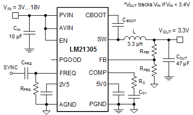
Typical Application Circuit

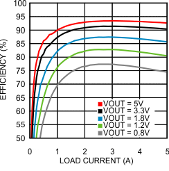
Typical Efficiency at 12 V, 500 kHz
