SNVS774Q May 2004 – June 2020 LM117 , LM317-N
PRODUCTION DATA.
- 1 Features
- 2 Applications
- 3 Description
- 4 Revision History
- 5 Device Comparison Table
- 6 Pin Configuration and Functions
- 7 Specifications
- 8 Detailed Description
-
9 Application and Implementation
- 9.1 Application Information
- 9.2
Typical Applications
- 9.2.1 1.25-V to 25-V Adjustable Regulator
- 9.2.2 5-V Logic Regulator With Electronic Shutdown
- 9.2.3 Slow Turnon 15-V Regulator
- 9.2.4 Adjustable Regulator With Improved Ripple Rejection
- 9.2.5 High Stability 10-V Regulator
- 9.2.6 High-Current Adjustable Regulator
- 9.2.7 Emitter-Follower Current Amplifier
- 9.2.8 1-A Current Regulator
- 9.2.9 Common-Emitter Amplifier
- 9.2.10 Low-Cost 3-A Switching Regulator
- 9.2.11 Current-Limited Voltage Regulator
- 9.2.12 Adjusting Multiple On-Card Regulators With Single Control
- 9.2.13 AC Voltage Regulator
- 9.2.14 12-V Battery Charger
- 9.2.15 Adjustable 4-A Regulator
- 9.2.16 Current-Limited 6-V Charger
- 9.2.17 Digitally Selected Outputs
- 10Power Supply Recommendations
- 11Layout
- 12Device and Documentation Support
- 13Mechanical, Packaging, and Orderable Information
11.1.1.2.2 Heatsinking the TO-263 (KTT) Package
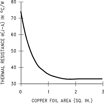
Figure 39 shows for the TO-263 the measured values of RθJA for different copper area sizes using a typical PCB with 1-oz. copper and no solder mask over the copper area used for heatsinking.
As shown in Figure 39, increasing the copper area beyond 1 square inch produces very little improvement. It must also be observed that the minimum value of RθJA for the TO-263 package mounted to a PCB is 32°C/W.
 Figure 39. RθJA vs Copper (1-oz.) Area for the TO-263 Package
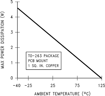
 As a design aid, Figure 40 shows the maximum allowable power dissipation compared to ambient temperature for the TO-263 device (assuming RθJA is 35°C/W and the maximum junction temperature is 125°C).
 Figure 40. Maximum Power Dissipation vs TAMB for the TO-263 Package