SNVS774Q May 2004 – June 2020 LM117 , LM317-N
PRODUCTION DATA.
- 1 Features
- 2 Applications
- 3 Description
- 4 Revision History
- 5 Device Comparison Table
- 6 Pin Configuration and Functions
- 7 Specifications
- 8 Detailed Description
-
9 Application and Implementation
- 9.1 Application Information
- 9.2
Typical Applications
- 9.2.1 1.25-V to 25-V Adjustable Regulator
- 9.2.2 5-V Logic Regulator With Electronic Shutdown
- 9.2.3 Slow Turnon 15-V Regulator
- 9.2.4 Adjustable Regulator With Improved Ripple Rejection
- 9.2.5 High Stability 10-V Regulator
- 9.2.6 High-Current Adjustable Regulator
- 9.2.7 Emitter-Follower Current Amplifier
- 9.2.8 1-A Current Regulator
- 9.2.9 Common-Emitter Amplifier
- 9.2.10 Low-Cost 3-A Switching Regulator
- 9.2.11 Current-Limited Voltage Regulator
- 9.2.12 Adjusting Multiple On-Card Regulators With Single Control
- 9.2.13 AC Voltage Regulator
- 9.2.14 12-V Battery Charger
- 9.2.15 Adjustable 4-A Regulator
- 9.2.16 Current-Limited 6-V Charger
- 9.2.17 Digitally Selected Outputs
- 10Power Supply Recommendations
- 11Layout
- 12Device and Documentation Support
- 13Mechanical, Packaging, and Orderable Information
11.1.1.2.3 Heatsinking the TO-252 (NDP) Package
If the maximum allowable value for RθJA is found to be ≥ 54°C/W (typical rated value) for the TO-252 package, no heatsink is needed because the package alone will dissipate enough heat to satisfy these requirements. If the calculated value for RθJA falls below these limits, a heatsink is required.
As a design aid, Table 1 shows the value of the RθJA of NDP the package for different heatsink area. The copper patterns that we used to measure these RθJAs are shown in Figure 45. Figure 41 reflects the same test results as what are in Table 1.
Figure 42 shows the maximum allowable power dissipation versus ambient temperature for the TO-252 device. Figure 43 shows the maximum allowable power dissipation versus copper area (in2) for the TO-252 device. See the AN-1028 Maximum Power Enhancement Techniques for Power Packages application note for thermal enhancement techniques to be used with SOT-223 and TO-252 packages.
Table 1. RθJA Different Heatsink Area
| LAYOUT | COPPER AREA | THERMAL RESISTANCE | |
|---|---|---|---|
| Top Side (in2)(1) | Bottom Side (in2) | (RθJA°C/W) TO-252 | |
| 1 | 0.0123 | 0 | 103 |
| 2 | 0.066 | 0 | 87 |
| 3 | 0.3 | 0 | 60 |
| 4 | 0.53 | 0 | 54 |
| 5 | 0.76 | 0 | 52 |
| 6 | 1.0 | 0 | 47 |
| 7 | 0.066 | 0.2 | 84 |
| 8 | 0.066 | 0.4 | 70 |
| 9 | 0.066 | 0.6 | 63 |
| 10 | 0.066 | 0.8 | 57 |
| 11 | 0.066 | 1.0 | 57 |
| 12 | 0.066 | 0.066 | 89 |
| 13 | 0.175 | 0.175 | 72 |
| 14 | 0.284 | 0.284 | 61 |
| 15 | 0.392 | 0.392 | 55 |
| 16 | 0.5 | 0.5 | 53 |
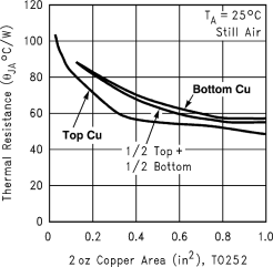 Figure 41. RθJA vs 2-oz. Copper Area for TO-252
 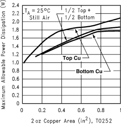 Figure 43. Maximum Allowable Power Dissipation vs 2-oz. Copper Area for TO-252
 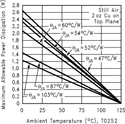 Figure 42. Maximum Allowable Power Dissipation vs Ambient Temperature for TO-252
 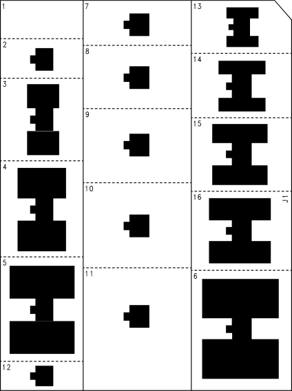 Figure 44. Top View of the Thermal Test Pattern in Actual Scale
 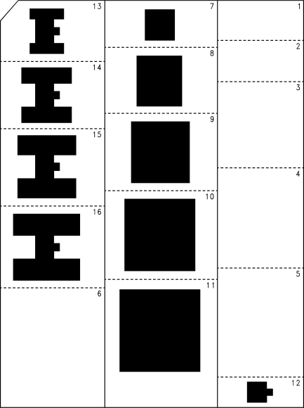 Figure 45. Bottom View of the Thermal Test Pattern in Actual Scale