SNVS774Q May   2004  – June 2020 LM117 , LM317-N

PRODUCTION DATA.  

  1. Features
  2. Applications
    1.     Typical Application
  3. Description
  4. Revision History
  5. Device Comparison Table
  6. Pin Configuration and Functions
    1.     Pin Functions, Metal Can Packages
    2.     Pin Functions
  7. Specifications
    1. 7.1 Absolute Maximum Ratings
    2. 7.2 ESD Ratings
    3. 7.3 Recommended Operating Conditions
    4. 7.4 Thermal Information, LM117
    5. 7.5 Thermal Information, LM317-N
    6. 7.6 LM117 Electrical Characteristics
    7. 7.7 LM317-N Electrical Characteristics
    8. 7.8 Typical Characteristics
  8. Detailed Description
    1. 8.1 Overview
    2. 8.2 Functional Block Diagram
    3. 8.3 Feature Description
      1. 8.3.1 Load Regulation
    4. 8.4 Device Functional Modes
      1. 8.4.1 External Capacitors
      2. 8.4.2 Protection Diodes
  9. Application and Implementation
    1. 9.1 Application Information
    2. 9.2 Typical Applications
      1. 9.2.1  1.25-V to 25-V Adjustable Regulator
        1. 9.2.1.1 Design Requirements
        2. 9.2.1.2 Detailed Design Procedure
        3. 9.2.1.3 Application Curve
      2. 9.2.2  5-V Logic Regulator With Electronic Shutdown
      3. 9.2.3  Slow Turnon 15-V Regulator
      4. 9.2.4  Adjustable Regulator With Improved Ripple Rejection
      5. 9.2.5  High Stability 10-V Regulator
      6. 9.2.6  High-Current Adjustable Regulator
      7. 9.2.7  Emitter-Follower Current Amplifier
      8. 9.2.8  1-A Current Regulator
      9. 9.2.9  Common-Emitter Amplifier
      10. 9.2.10 Low-Cost 3-A Switching Regulator
      11. 9.2.11 Current-Limited Voltage Regulator
      12. 9.2.12 Adjusting Multiple On-Card Regulators With Single Control
      13. 9.2.13 AC Voltage Regulator
      14. 9.2.14 12-V Battery Charger
      15. 9.2.15 Adjustable 4-A Regulator
      16. 9.2.16 Current-Limited 6-V Charger
      17. 9.2.17 Digitally Selected Outputs
  10. 10Power Supply Recommendations
  11. 11Layout
    1. 11.1 Layout Guidelines
      1. 11.1.1 Thermal Considerations
        1. 11.1.1.1 Heatsink Requirements
        2. 11.1.1.2 Heatsinking Surface Mount Packages
          1. 11.1.1.2.1 Heatsinking the SOT-223 (DCY) Package
          2. 11.1.1.2.2 Heatsinking the TO-263 (KTT) Package
          3. 11.1.1.2.3 Heatsinking the TO-252 (NDP) Package
    2. 11.2 Layout Examples
  12. 12Device and Documentation Support
    1. 12.1 Documentation Support
      1. 12.1.1 Related Documentation
    2. 12.2 Related Links
    3. 12.3 Receiving Notification of Documentation Updates
    4. 12.4 Support Resources
    5. 12.5 Trademarks
    6. 12.6 Electrostatic Discharge Caution
    7. 12.7 Glossary
  13. 13Mechanical, Packaging, and Orderable Information

封装选项

机械数据 (封装 | 引脚)
散热焊盘机械数据 (封装 | 引脚)
订购信息

Current-Limited Voltage Regulator

A maximum limit on output current can be set using the circuit shown in Figure 29. The load current travels through R3 and R4. As the load current increases, the voltage drop across R3 increases until the NPN transistor is driven, during which the ADJ pin is pulled down to ground and the output voltage is pulled down to the reference voltage of 1.25 V.
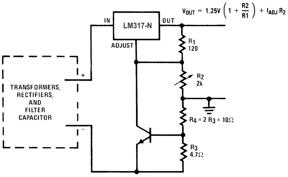
LM117 LM317-N 906323.gif
LM117 LM317-N new_eq_1.gif
(Compared to LM117's higher current limit)
—At 50 mA output only ¾ volt of drop occurs in R3 and R4
Figure 29. Current-Limited Voltage Regulator