ZHCS029E January 2011 – August 2023 ISO3086T
PRODUCTION DATA
- 1
- 1 特性
- 2 应用
- 3 说明
- 4 Revision History
- 5 Pin Configuration and Functions
-
6 Specifications
- 6.1 Absolute Maximum Ratings
- 6.2 ESD Ratings
- 6.3 Recommended Operating Conditions
- 6.4 Thermal Information
- 6.5 Power Ratings
- 6.6 Insulation Specifications
- 6.7 Safety-Related Certifications
- 6.8 Safety Limiting Values
- 6.9 Electrical Characteristics: Driver
- 6.10 Electrical Characteristics: Receiver
- 6.11 Transformer Driver Characteristics
- 6.12 Supply Current
- 6.13 Switching Characteristics: Driver
- 6.14 Switching Characteristics: Receiver
- 6.15 Insulation Characteristics Curves
- 6.16 Typical Characteristics
- 7 Parameter Measurement Information
- 8 Detailed Description
- 9 Application and Implementation
- 10Power Supply Recommendations
- 11Layout
- 12Device and Documentation Support
- 13Mechanical, Packaging, and Orderable Information
5 Pin Configuration and Functions
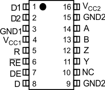
 Figure 5-1 DW Package16-Pin SOICTop View
Table 5-1 Pin Functions
| PIN | I/O | DESCRIPTION | |
|---|---|---|---|
| NAME | NO. | ||
| A | 14 | I | Non-inverting Receiver Input |
| B | 13 | I | Inverting Receiver Input |
| D1 | 1 | O | Transformer Driver Terminal 1, Open Drain Output |
| D2 | 2 | O | Transformer Driver Terminal 2, Open Drain Output |
| D | 8 | I | Driver Input |
| DE | 7 | I | Driver Enable Input |
| GND1 | 3 | — | Logic-side Ground |
| GND2 | 9, 15 | — | Bus-side Ground. Both pins are internally connected. |
| NC | 10 | — | No Connect. This pin is not connected to any internal circuitry. |
| R | 5 | O | Receiver Output |
| RE | 6 | I | Receiver Enable Input. This pin has complementary logic. |
| VCC1 | 4 | — | Logic-side Power Supply |
| VCC2 | 16 | — | Bus-side Power Supply |
| Y | 11 | O | Non-inverting Driver Output |
| Z | 12 | O | Inverting Driver Output |