ZHCSK07A July 2019 – January 2021 INA253-Q1
PRODUCTION DATA
- 1 特性
- 2 应用
- 3 说明
- 4 Revision History
- 5 Pin Configuration and Functions
- 6 Specifications
-
7 Detailed Description
- 7.1 Overview
- 7.2 Functional Block Diagram
- 7.3 Feature Description
- 7.4
Device Functional Modes
- 7.4.1 Adjusting the Output Midpoint With the Reference Pins
- 7.4.2 Reference Pin Connections for Unidirectional Current Measurements
- 7.4.3 Ground Referenced Output
- 7.4.4 Reference Pin Connections for Bidirectional Current Measurements
- 7.4.5 Output Set to Mid-Supply Voltage
- 7.4.6 Output Set to Mid-External Reference
- 7.4.7 Output Set Using Resistor Divide
- 8 Application and Implementation
- 9 Power Supply Recommendations
- 10Layout
- 11Device and Documentation Support
- 12Mechanical, Packaging, and Orderable Information
7.4.4.1 Output Set to External Reference Voltage
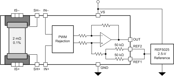
Connecting both pins together and then to a reference voltage results in an output voltage equal to the reference voltage for the condition of shorted input pins or a 0-V differential input. Figure 7-7 shows this configuration. The output voltage decreases below the reference voltage when the IN+ pin is negative relative to the IN– pin, and increases when the IN+ pin is positive relative to the IN– pin. This technique is the most accurate way to bias the output to a precise voltage.
 Figure 7-7 External Reference Output