ZHCSK07A July 2019 – January 2021 INA253-Q1
PRODUCTION DATA
- 1 特性
- 2 应用
- 3 说明
- 4 Revision History
- 5 Pin Configuration and Functions
- 6 Specifications
-
7 Detailed Description
- 7.1 Overview
- 7.2 Functional Block Diagram
- 7.3 Feature Description
- 7.4
Device Functional Modes
- 7.4.1 Adjusting the Output Midpoint With the Reference Pins
- 7.4.2 Reference Pin Connections for Unidirectional Current Measurements
- 7.4.3 Ground Referenced Output
- 7.4.4 Reference Pin Connections for Bidirectional Current Measurements
- 7.4.5 Output Set to Mid-Supply Voltage
- 7.4.6 Output Set to Mid-External Reference
- 7.4.7 Output Set Using Resistor Divide
- 8 Application and Implementation
- 9 Power Supply Recommendations
- 10Layout
- 11Device and Documentation Support
- 12Mechanical, Packaging, and Orderable Information
7.3.1 Integrated Shunt Resistor
The INA253-Q1 features a precise, low-drift, current-sensing resistor that provides accurate measurements over the entire specified temperature range of –40 °C to +125 °C. The integrated current-sensing resistor provides measurement stability over temperature, and simplifies printed circuit board (PCB) layout and board constraint difficulties common in high-precision measurements.
The onboard current-sensing resistor is designed as a 4-wire (or Kelvin) connected resistor that enables accurate measurements through a force-sense connection. Connecting the amplifier inputs pins (VIN– and VIN+) to the sense pins of the shunt resistor (SH– and SH+) eliminates many of the parasitic impedances commonly found in typical very-low sensing-resistor level measurements. Although the sense connection of the current-sensing resistor can be accessed through the SH+ and SH– pins, this resistor is not intended to be used as a stand-alone component. The INA253-Q1 is system-calibrated to makes sure that the current-sensing resistor and current-sensing amplifier are both precisely matched to one another. Use of the shunt resistor without the onboard amplifier results in a current-sensing resistor tolerance of approximately 5%. To achieve the optimized system gain specification, the onboard sensing resistor must be used with the internal current-sensing amplifier.
The INA253-Q1 has approximately 4.5 mΩ of package resistance. Of this total package resistance, 2 mΩ is a precisely-controlled resistance from the Kelvin-connected current-sensing resistor used by the amplifier. The power dissipation requirements of the system and package are based on the total 4.5-mΩ package resistance between the IS+ and IS– pins. The heat dissipated across the package when current flows through the device ultimately determines the maximum current that can be safely handled by the package. The current consumption of the silicon is relatively low, leaving the total package resistance to carry the high load current as the primary contributor to the total power dissipation of the package. The maximum safe-operating current level is set to make sure that the heat dissipated across the package is limited so that no damage occurs to the resistor or the package, or that the internal junction temperature of the silicon does not exceed a 150 °C limit.
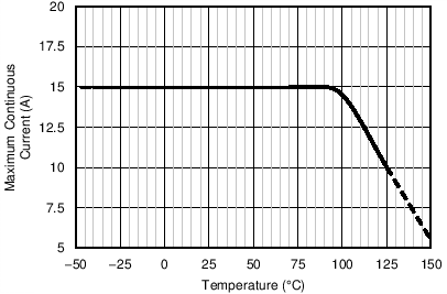
External factors, such as ambient temperature, external air flow, and PCB layout, contribute to how effectively the device dissipates heat. The internal heat is developed as a result of the current flowing through the total package resistance of 4.5 mΩ. Under the conditions of no air flow, a maximum ambient temperature of 85 °C, and 1-oz. copper input power planes, the INA253-Q1 accommodates continuous current levels up to 15 A. Figure 7-1 shows that the current-handling capability is derated at temperatures greater than the 85 °C level, with safe operation up to 10 A at a 125 °C ambient temperature. With air flow and larger 2-oz. copper input power planes, the INA253-Q1 safely accommodates continuous current levels up to 15 A across the entire –40 °C to +125 °C temperature range.
 Figure 7-1 Maximum Continuous Current vs Temperature