ZHCSCV7 August 2014 DRV8833C
PRODUCTION DATA.
- 1 特性
- 2 应用
- 3 说明
- 4 修订历史记录
- 5 Pin Configuration and Functions
- 6 Specifications
- 7 Detailed Description
- 8 Application and Implementation
- 9 Power Supply Recommendations
- 10Layout
- 11器件和文档支持
- 12机械封装和可订购信息
封装选项
机械数据 (封装 | 引脚)
散热焊盘机械数据 (封装 | 引脚)
- RTE|16
订购信息
7 Detailed Description
7.1 Overview
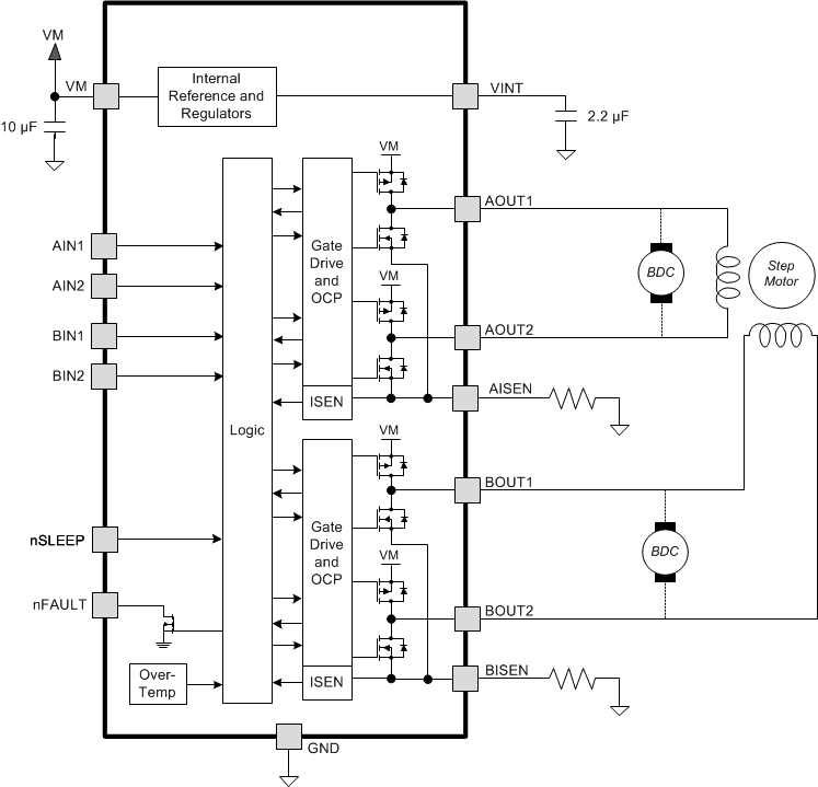
The DRV8833C device is an integrated motor driver solution for brushed DC or bipolar stepper motors. The device integrates two PMOS + NMOS H-bridges and current regulation circuitry. The DRV8833C can be powered with a supply voltage from 2.7 to 10.8 V and can provide an output current up to 700 mA RMS.
A simple PWM interface allows easy interfacing to the controller circuit.
The current regulation is a 20-µs fixed off-time slow decay.
The device includes a low-power sleep mode, which lets the system save power when not driving the motor.
7.2 Functional Block Diagram
7.3 Feature Description
7.3.1 PWM Motor Drivers
The DRV8833C contains drivers for two full H-bridges. Figure 6 shows a block diagram of the circuitry.
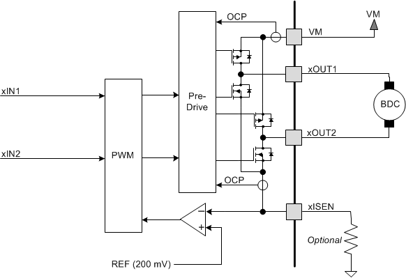 Figure 6. H-Bridge and Current-Chopping Circuitry
7.3.2 Bridge Control and Decay Modes
The AIN1 and AIN2 input pins control the state of the AOUT1 and AOUT2 outputs; similarly, the BIN1 and BIN2 input pins control the state of the BOUT1 and BOUT2 outputs (see Table 1).
Table 1. H-Bridge Logic
| xIN1 | xIN2 | xOUT1 | xOUT2 | FUNCTION |
|---|---|---|---|---|
| 0 | 0 | Z | Z | Coast / fast decay |
| 0 | 1 | L | H | Reverse |
| 1 | 0 | H | L | Forward |
| 1 | 1 | L | L | Brake / slow decay |
The inputs can also be used for PWM control of the motor speed. When controlling a winding with PWM and the drive current is interrupted, the inductive nature of the motor requires that the current must continue to flow (called recirculation current). To handle this recirculation current, the H-bridge can operate in two different states, fast decay or slow decay. In fast-decay mode, the H-bridge is disabled and recirculation current flows through the body diodes. In slow-decay mode, the motor winding is shorted by enabling both low-side FETs.
To externally pulse-width modulate the bridge in fast-decay mode, the PWM signal is applied to one xIN pin while the other is held low; to use slow-decay mode, one xIN pin is held high. See Table 2 for more information.
Table 2. PWM Control of Motor Speed
| xIN1 | xIN2 | FUNCTION |
|---|---|---|
| PWM | 0 | Forward PWM, fast decay |
| 1 | PWM | Forward PWM, slow decay |
| 0 | PWM | Reverse PWM, fast decay |
| PWM | 1 | Reverse PWM, slow decay |
The internal current control is still enabled when applying external PWM to xIN. To disable the current control when applying external PWM, the xISEN pins should be connected directly to ground. Figure 7 show the current paths in different drive and decay modes.
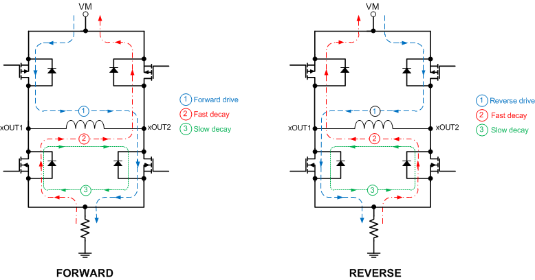 Figure 7. Drive and Decay Modes
7.3.3 Current Control
The current through the motor windings may be limited, or controlled, by a 20-µs constant off-time PWM current regulation, or current chopping. For DC motors, current control is used to limit the start-up and stall current of the motor. For stepper motors, current control is often used at all times.
When an H-bridge is enabled, current rises through the winding at a rate dependent on the DC voltage and inductance of the winding. If the current reaches the current chopping threshold, the bridge disables the current until the beginning of the next PWM cycle. Note that immediately after the output is enabled, the voltage on the xISEN pin is ignored for a fixed period of time before enabling the current sense circuitry. This blanking time is fixed at 3.75 μs.
The PWM chopping current is set by a comparator that compares the voltage across a current sense resistor connected to the xISEN pins with a reference voltage. The reference voltage, VTRIP, is is fixed at 200 mV nominally.
The chopping current is calculated as in Equation 1.
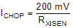
Example: If a 1-Ω sense resistor is used, the chopping current will be 200 mV / 1 Ω = 200 mA.
NOTE
If current control is not needed, the xISEN pins should be connected directly to ground.
7.3.4 Decay Mode
After the chopping current threshold is reached, the H-bridge switches to slow-decay mode. This state is held for toff (20 µs) until the next cycle to turn on the high-side MOSFETs.
7.3.5 Slow Decay
In slow-decay mode, the high-side MOSFETs are turned off and both of the low-side MOSFETs are turned on. The motor current decreases while flowing in the two low-side MOSFETs until reaching its fixed off time (typically 20 µs). After that, the high-side MOSFETs are enabled to increase the winding current again.
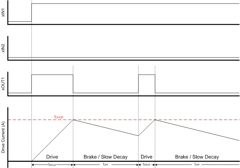 Figure 8. Current Chopping Operation
7.3.6 Sleep Mode
Driving nSLEEP low puts the device into a low-power sleep state. In this state, the H-bridges are disabled, all internal logic is reset, and all internal clocks are stopped. All inputs are ignored until nSLEEP returns inactive high. When returning from sleep mode, some time, tWAKE, needs to pass before the motor driver becomes fully operational. To make the board design simple, the nSLEEP can be pulled up to the supply (VM). TI recommends to use a pullup resistor when this is done. This resistor limits the current to the input in case VM is higher than 6.5 V. Internally, the nSLEEP pin has a 500-kΩ resistor to GND. It also has a clamping Zener diode that clamps the voltage at the pin at 6.5 V. Currents greater than 250 µA can cause damage to the input structure. Therefore, TI recommends a pullup resistor between 20 to 75 kΩ.
7.3.7 Parallel Mode
The two H-bridges in the DRV8833C can be connected in parallel for double the current of a single H-bridge. The internal dead time in the DRV8833C prevents any risk of cross-conduction (shoot-through) between the two bridges due to timing differences between the two bridges. Figure 9 shows the connections.
 Figure 9. Parallel Mode Schematic
7.3.8 Protection Circuits
The DRV8833C is fully protected against overcurrent, overtemperature, and undervoltage events.
7.3.8.1 Overcurrent Protection (OCP)
An analog current limit (IOCP) circuit on each FET limits the current through the FET by limiting the gate drive. If this analog current limit persists for longer than the OCP deglitch time (tDEG), all FETs in the H-bridge are disabled and the nFAULT pin is driven low. The driver is re-enabled after the OCP retry period (tOCP) has passed. nFAULT becomes high again after the retry time. If the fault condition is still present, the cycle repeats. If the fault is no longer present, normal operation resumes and nFAULT remains deasserted. Note that only the H-bridge in which the OCP is detected will be disabled while the other bridge functions normally.
Overcurrent conditions are detected independently on both high-side and low-side devices; a short to ground, supply, or across the motor winding all result in an overcurrent shutdown. Note that overcurrent protection does not use the current sense circuitry used for PWM current control, so it functions even without presence of the xISEN resistors.
7.3.8.2 Thermal Shutdown (TSD)
If the die temperature exceeds safe limits, all FETs in the H-bridge are disabled and the nFAULT pin is driven low. After the die temperature has fallen below the specified hysteresis (THYS), operation automatically resumes. The nFAULT pin is released after operation has resumed.
7.3.8.3 UVLO
If at any time the voltage on the VM pin falls below the UVLO threshold voltage, VUVLO, all circuitry in the device is disabled, and all internal logic is reset. Operation resumes when VM rises above the UVLO threshold. The nFAULT pin is not driven low during an undervoltage condition.
Table 3. Device Protection
| Fault | Condition | Error Report | H-Bridge | Internal Circuits | Recovery |
|---|---|---|---|---|---|
| VM undervoltage (UVLO) | VM < 2.6 V | None | Disabled | Disabled | VM > 2.7 V |
| Overcurrent (OCP) | IOUT > IOCP | FAULTn | Disabled | Operating | OCP |
| Thermal Shutdown (TSD) | TJ > TTSD | FAULTn | Disabled | Operating | TJ < TTSD – THYS |
7.4 Device Functional Modes
The DRV8833C is active unless the nSLEEP pin is brought logic low. In sleep mode, the H-bridge FETs are disabled (Hi-Z). Note that tSLEEP must elapse after a falling edge on the nSLEEP pin before the device is in sleep mode. The DRV8833C is brought out of sleep mode automatically if nSLEEP is brought logic high. Note that tWAKE must elapse before the outputs change state after wake-up.
Table 4. Modes of Operation
| Fault | Condition | H-Bridge | Internal Circuits |
|---|---|---|---|
| Operating | nSLEEP pin high | Operating | Operating |
| Sleep mode | nSLEEP pin low | Disabled | Disabled |
| Fault encountered | Any fault condition met | Disabled | See Table 3 |