ZHCSCV7 August 2014 DRV8833C
PRODUCTION DATA.
- 1 特性
- 2 应用
- 3 说明
- 4 修订历史记录
- 5 Pin Configuration and Functions
- 6 Specifications
- 7 Detailed Description
- 8 Application and Implementation
- 9 Power Supply Recommendations
- 10Layout
- 11器件和文档支持
- 12机械封装和可订购信息
封装选项
机械数据 (封装 | 引脚)
散热焊盘机械数据 (封装 | 引脚)
- RTE|16
订购信息
6 Specifications
6.1 Absolute Maximum Ratings
over operating free-air temperature (unless otherwise noted) (1)| MIN | MAX | UNIT | ||
|---|---|---|---|---|
| Voltage | Power supply (VM) | –0.3 | 11.8 | V |
| Internal regulator (VINT) | –0.3 | 3.8 | V | |
| Control pins (AIN1, AIN2, BIN1, BIN2, nSLEEP, nFAULT) | –0.3 | 7 | V | |
| Continuous phase node pins (AOUT1, AOUT2, BOUT1, BOUT2) | –0.3 | VM + 0.5 | V | |
| Pulsed 10 µs phase node pins (AOUT1, AOUT2, BOUT1, BOUT2) | –1 | VM + 1 | V | |
| Continuous shunt amplifier input pins (AISEN, BISEN) | –0.3 | 0.5 | V | |
| Pulsed 10 µs shunt amplifier input pins (AISEN, BISEN) | –1 | 1 | V | |
| Peak drive current (AOUT1, AOUT2, BOUT1, BOUT2, AISEN, BISEN) | Internally limited | A | ||
| TJ | Operating junction temperature | –40 | 150 | °C |
(1) Stresses beyond those listed under Absolute Maximum Ratings may cause permanent damage to the device. These are stress ratings only, which do not imply functional operation of the device at these or any other conditions beyond those indicated under Recommended Operating Conditions. Exposure to absolute-maximum-rated conditions for extended periods may affect device reliability.
6.2 Handling Ratings
| MIN | MAX | UNIT | |||
|---|---|---|---|---|---|
| Tstg | Storage temperature range | –65 | 150 | °C | |
| V(ESD) | Electrostatic discharge | Human body model (HBM), per ANSI/ESDA/JEDEC JS-001, all pins(1) | –2000 | 2000 | V |
| Charged device model (CDM), per JEDEC specification JESD22-C101, all pins(2) | –1000 | 1000 | |||
(1) JEDEC document JEP155 states that 500-V HBM allows safe manufacturing with a standard ESD control process.
(2) JEDEC document JEP157 states that 250-V CDM allows safe manufacturing with a standard ESD control process.
6.3 Recommended Operating Conditions
over operating free-air temperature range (unless otherwise noted)| MIN | MAX | UNIT | |||
|---|---|---|---|---|---|
| VM | Power supply voltage range(1) | 2.7 | 10.8 | V | |
| VI | Logic level input voltage | 0 | 5.5 | V | |
| IRMS | Motor RMS current(2) | PWP package | 0 | 0.7 | A |
| RTE package | 0 | 0.6 | A | ||
| ƒPWM | Applied PWM signal to AIN1, AIN2, BIN1, or BIN2 | 0 | 200 | kHz | |
| TA | Operating ambient temperature | –40 | 85 | °C | |
(1) Note that when VM is below 5 V, RDS(ON) increases and maximum output current is reduced.
(2) Power dissipation and thermal limits must be observed.
6.4 Thermal Information
| THERMAL METRIC(1) | DRV8833C | UNIT | ||
|---|---|---|---|---|
| HTSSOP | QFN | |||
| 16 PINS | 16 PINS | |||
| RθJA | Junction-to-ambient thermal resistance | 40.5 | 44.7 | °C/W |
| RθJC(top) | Junction-to-case (top) thermal resistance | 32.9 | 48.5 | |
| RθJB | Junction-to-board thermal resistance | 28.8 | 16.8 | |
| ψJT | Junction-to-top characterization parameter | 0.6 | 0.7 | |
| ψJB | Junction-to-board characterization parameter | 11.5 | 16.7 | |
| RθJC(bot) | Junction-to-case (bottom) thermal resistance | 4.8 | 4.2 | |
(1) For more information about traditional and new thermal metrics, see the IC Package Thermal Metrics application report, SPRA953.
6.5 Electrical Characteristics
over operating free-air temperature range (unless otherwise noted)| PARAMETER | TEST CONDITIONS | MIN | TYP | MAX | UNIT | |
|---|---|---|---|---|---|---|
| POWER SUPPLIES (VM, VINT) | ||||||
| VM | VM operating voltage | 2.7 | 10.8 | V | ||
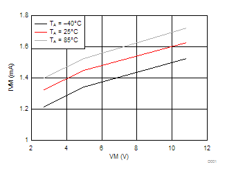
| IVM | VM operating supply current | VM = 5 V, xINx low, nSLEEP high | 1.7 | 3 | mA | |
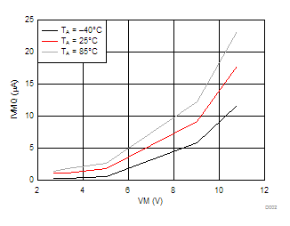
| IVMQ | VM sleep mode supply current | VM = 5 V, nSLEEP low | 1.6 | 2.7 | μA | |
| tSLEEP | Sleep time | nSLEEP low to sleep mode | 10 | µs | ||
| tWAKE | Wake-up time | nSLEEP high to output transition | 155 | μs | ||
| tON | Turn-on time | VM > VUVLO to output transition | 25 | μs | ||
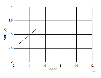
| VINT | Internal regulator voltage | VM = 5 V | 3 | 3.3 | 3.6 | V |
| CONTROL INPUTS (AIN1, AIN2, BIN1, BIN2, nSLEEP) | ||||||
| VIL | Input logic low voltage | xINx | 0 | 0.7 | V | |
| nSLEEP | 0 | 0.5 | ||||
| VIH | Input logic high voltage | xINx | 2 | 5.5 | V | |
| nSLEEP | 2.5 | 5.5 | ||||
| VHYS | Input logic hysteresis | 350 | 400 | 650 | mV | |
| IIL | Input logic low current | VIN = 0 V | –1 | 1 | μA | |
| IIH | Input logic high current | VIN = 5 V | 50 | μA | ||
| RPD | Pulldown resistance | xINx | 100 | 150 | 250 | kΩ |
| nSLEEP | 380 | 500 | 750 | |||
| tDEG | Input deglitch time | 575 | ns | |||
| tPROP | Propagation delay INx to OUTx | VM = 5 V | 1.2 | μs | ||
| CONTROL OUTPUTS (nFAULT) | ||||||
| VOL | Output logic low voltage | IO = 5 mA | 0.5 | V | ||
| IOH | Output logic high leakage | RPULLUP = 1 kΩ to 5 V | –1 | 1 | μA | |
| MOTOR DRIVER OUTPUTS (AOUT1, AOUT2, BOUT1, BOUT2) | ||||||
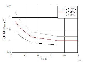
| RDS(ON) | High-side FET on-resistance | VM = 5 V, I = 0.2 A, TA = 25°C | 1180 | mΩ | ||
| VM = 5 V, I = 0.2 A, TA = 85°C(1) | 1400 | 1475 | ||||
| VM = 2.7 V, I = 0.2 A, TA = 25°C | 1550 | |||||
| VM = 2.7 V, I = 0.2 A, TA = 85°C(1) | 1875 | 1975 | ||||
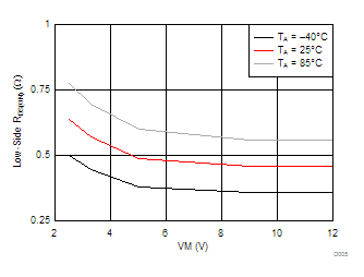
| RDS(ON) | Low-side FET on-resistance | VM = 5 V, I = 0.2 A, TA = 25°C | 555 | mΩ | ||
| VM = 5 V, I = 0.2 A, TA = 85°C(1) | 675 | 705 | ||||
| VM = 2.7 V, I = 0.2 A, TA = 25°C | 635 | |||||
| VM = 2.7 V, I = 0.2 A, TA = 85°C(1) | 775 | 815 | ||||
| IOFF | Off-state leakage current | VM = 5 V | –1 | 1 | μA | |
| tRISE | Output rise time | VM = 5 V; RL = 16 Ω to GND | 70 | ns | ||
| tFALL | Output fall time | VM = 5 V; RL = 16 Ω to VM | 80 | ns | ||
| tDEAD | Output dead time | Internal dead time | 450 | ns | ||
| PWM CURRENT CONTROL (AISEN, BISEN) | ||||||
| VTRIP | xISEN trip voltage | 160 | 200 | 240 | mV | |
| tOFF | Current control constant off time | Internal PWM constant off time | 20 | µs | ||
| PROTECTION CIRCUITS | ||||||
| VUVLO | VM undervoltage lockout | VM falling; UVLO report | 2.6 | V | ||
| VM rising; UVLO recovery | 2.7 | |||||
| VUVLO,HYS | VM undervoltage hysteresis | Rising to falling threshold | 90 | mV | ||
| IOCP | Overcurrent protection trip level | 1 | A | |||
| tDEG | Overcurrent deglitch time | 2.3 | μs | |||
| tOCP | Overcurrent protection period | 1.4 | ms | |||
| TTSD(1) | Thermal shutdown temperature | Die temperature, TJ | 150 | °C | ||
| THYS | Thermal shutdown hysteresis | Die temperature, TJ | 20 | °C | ||
(1) Not tested in production; based on design and characterization data
6.6 Typical Characteristics