ZHCSCV7 August 2014 DRV8833C
PRODUCTION DATA.
- 1 特性
- 2 应用
- 3 说明
- 4 修订历史记录
- 5 Pin Configuration and Functions
- 6 Specifications
- 7 Detailed Description
- 8 Application and Implementation
- 9 Power Supply Recommendations
- 10Layout
- 11器件和文档支持
- 12机械封装和可订购信息
封装选项
机械数据 (封装 | 引脚)
散热焊盘机械数据 (封装 | 引脚)
- RTE|16
订购信息
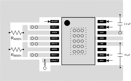
10 Layout
10.1 Layout Guidelines
Bypass the VM terminal to GND using a low-ESR ceramic bypass capacitor with a recommended value of 10 µF rated for VM. This capacitor should be placed as close to the VM pin as possible with a thick trace or ground plane connection to the device GND pin and PowerPAD.
Bypass VINT to ground with a ceramic capacitor rated 6.3 V. Place this bypassing capacitor as close to the pin as possible.
10.2 Layout Example