SLVS854E July 2008 – December 2014 DRV8809
PRODUCTION DATA.
- 1 Features
- 2 Applications
- 3 Description
- 4 Revision History
- 5 Pin Configuration and Functions
- 6 Specifications
-
7 Detailed Description
- 7.1 Overview
- 7.2 Functional Block Diagram
- 7.3
Feature Description
- 7.3.1
Serial Interface
- 7.3.1.1 Setup Mode/Power-Down Mode
- 7.3.1.2 Extended Setup Mode
- 7.3.1.3 Serial Interface Timing
- 7.3.1.4 Bipolar Current Regulated Stepper Motor Drive
- 7.3.1.5 Short/Open for Motor Outputs
- 7.3.1.6 DCDC_MODE for Parallel-Mode Control
- 7.3.1.7 DCDC_MODE and C_SELECT Timing Delay and Start-Up Order
- 7.3.1.8 In-Reset: Input for System Reset
- 7.3.1.9 Blanking Time Insertion Timing for DC Motor Driving
- 7.3.2 Motor Driver Configuration
- 7.3.3 Charge Pump
- 7.3.1
Serial Interface
- 7.4 Device Functional Modes
- 7.5 Register Maps
- 8 Application and Implementation
- 9 Power Supply Recommendations
- 10Layout
- 11Device and Documentation Support
- 12Mechanical, Packaging, and Orderable Information
6 Specifications
6.1 Absolute Maximum Ratings
over operating free-air temperature range (unless otherwise noted)| MIN | MAX | UNIT | ||
|---|---|---|---|---|
| VM | Supply voltage(1) | 50 | V | |
| Logic input voltage range, serial I/F inputs, and reset (2) | –0.3 | 5.5 | V | |
| Continuous total power dissipation (θJA = 20°C/W) | 4 | W | ||
| Continuous motor-drive output current for each H-bridge (100 ms) | 3 | A | ||
| Peak motor-drive output current for each H-bridge (500 ns) | 8 | A | ||
| Continuous DC-DC converter output current | 1.5 | A | ||
| Continuous DC-DC converter output current ODB, C in parallel mode | 3.0 | A | ||
| TJ | Operating junction temperature range (1 h) | 0 | 150 | °C |
| Lead temperature 1.6 mm (1/16 in) from case for 10 s | 260 | °C |
(1) Stresses beyond those listed under Absolute Maximum Ratings may cause permanent damage to the device. These are stress ratings only and functional operation of the device at these or any other conditions beyond those indicated under Recommended Operating Conditions is not implied. Exposure to absolute-maximum-rated conditions for extended periods may affect device reliability.
(2) The negative spike less than –5 V and narrower than 50-ns duration should not cause any problem.
6.2 Handling Ratings
| MIN | MAX | UNIT | |||
|---|---|---|---|---|---|
| Tstg | Storage temperature range | –65 | 150 | °C | |
| V(ESD) | Electrostatic discharge | Human body model (HBM), per ANSI/ESDA/JEDEC JS-001, all pins(1) | -2 | 2 | kV |
| Charged device model (CDM), per JEDEC specification JESD22-C101, all pins(2) | -500 | 500 | V | ||
(1) JEDEC document JEP155 states that 500-V HBM allows safe manufacturing with a standard ESD control process.
(2) JEDEC document JEP157 states that 250-V CDM allows safe manufacturing with a standard ESD control process.
6.3 Recommended Operating Conditions
| MIN | NOM | MAX | UNIT | |
|---|---|---|---|---|
| Supply voltage, VM for motor control | 18 | 27 | 40 | V |
| Supply voltage for DC-DC converter (VDIN)(2) | 7 | 27 | 40 | V |
| Average output current for motor driver for each H-bridge | 800 | mA | ||
| DC output current for DC-DC converter | 1.2 | A | ||
| DC output current for DC-DC in Ch-B/C parallel mode | 2.4 | A | ||
| Operating ambient temperature(1) | –40 | 50 | °C | |
| Operating junction temperature | 0 | 120 | °C |
(1) If the total power is less than 4 W, then the operating ambient temperature range is -40°C to 60°C.
(2) VDIN should be connected to VM externally.
6.4 Thermal Information
| THERMAL METRIC(1) | DRV8809 | UNIT | |
|---|---|---|---|
| HTQFP | |||
| 64 PINS | |||
| RθJA | Junction-to-ambient thermal resistance | 26.2 | °C/W |
| RθJC(top) | Junction-to-case (top) thermal resistance | 12.6 | |
| RθJB | Junction-to-board thermal resistance | 10.4 | |
| ψJT | Junction-to-top characterization parameter | 0.3 | |
| ψJB | Junction-to-board characterization parameter | 10.3 | |
| RθJC(bot) | Junction-to-case (bottom) thermal resistance | 0.5 | |
(1) For more information about traditional and new thermal metrics, see the IC Package Thermal Metrics application report, SPRA953.
6.5 Electrical Characteristics
TJ = 0°C to 120°C, VM = 7 V to 40 V (unless otherwise noted)| PARAMETER | TEST CONDITIONS | MIN | TYP | MAX | UNIT | ||
|---|---|---|---|---|---|---|---|
| SUPPLY (SLEEP) CURRENT | |||||||
| ISLEEP1 | Supply (sleep) current 1 | nSLEEP = L, DC-DC all off | 4 | 5 | mA | ||
| ISLEEP2 | Supply (sleep) current 2 | nSLEEP = L, VM = 8 V, Full duty cycle | 7 | 10 | mA | ||
| ISLEEP3 | Supply (sleep) current 3 | nSLEEP = L, VM = 40 V, Full duty cycle | 8 | 10 | mA | ||
| DIGITAL INTERFACE CIRCUIT | |||||||
| VIH | Digital high-level input voltage | Digital inputs(1) | 2 | 5 | V | ||
| IIH | Digital high-level input current | Digital inputs | 100 | μA | |||
| VIL | Digital low-level input voltage | Digital inputs | 0.8 | V | |||
| IIL | Digital low-level input current | Digital inputs | 100 | μA | |||
| Vhys | Digital input hysteresis | Digital inputs | 0.3 | 0.45 | 0.6 | V | |
| Tdegl | Digital input deglitch time | In-Reset | 2.5 | 7.5 | μs | ||
| CHARGE-PUMP VCP (CP = 0.1 μF to 0.47 μF, Cbk = 0.01 μF ± 10%) | |||||||
| VO(CP) | Output voltage | ILOAD = 0 mA, | VM > VthVM2 | VM + 10 | VM + 13 | V | |
| f(CP) | Switching frequency | 1.6 | MHz | ||||
| tstart | Start-up time | CStorage = 0.1 μF, | VM ≥ 16 V | 0.5 | 2 | ms | |
| INTERNAL CLOCK OSCI | |||||||
| fOSCi | System clock frequency | 5.76 | 6.4 | 7.04 | MHz | ||
| VREF INPUT | |||||||
| VREF | Reference voltage input | 0.8 | 2.5 | 3.6 | V | ||
| Ileak-vr | Input leak current | 1 | μA | ||||
| C_SELECT FOR DC-DC START-UP SELECTION (DCDC_MODE = L) | |||||||
| Vcs0 | DC-DC all off | 0 | 0.3 | V | |||
| Vcs1 | DC-DC all off | Pull down by external 200-kΩ resistor | 1.3 | 2 | V | ||
| Vcs2 | Turn on ODA then ODB and ODC |
As pin open | 3 | 3.3 | V | ||
| C_SELECT FOR DC-DC START-UP SELECTION (DCDC_MODE = H OR OPEN, CH-B/C PARALLEL MODE) | |||||||
| Vcs0 | DC-DC all off | 0 | 0.3 | V | |||
| Vcs1 | Turn on ODB/C then ODA | Pull down by external 200-kΩ resistor | 1.3 | 2 | V | ||
| Vcs2 | Turn on ODA then ODB/C | As pin open | 3 | 3.6 | V | ||
| THREE DC-DC CONVERTERS(2) | |||||||
| VDINOPE | Operating supply voltage | Ratio to VOUT(DC) | 1.25 = VO | V | |||
| ODA ODB ODC |
VoutA = 1.5 V – 30 V, VoutB/C = 1.5 V – 10 V, Programmable with external reference on FBX × VDIN > 1.25 × Vout (largest) |
20 V ≤ VDIN < 40 V | –3% | VO | 3% | ||
| 6.5 V ≤ VDIN < 20 V | –3% | VO | 5% | ||||
| VthVM– < VDIN < 6.5 V, | VO ≤ 3.3 V | –3% | VO | 5% | |||
| VFB | FBX feedback voltage | For ODA/B/C | 1.50 | V | |||
| IO ODx | ODx output current (dc) | With external L and C | 1.5 | A | |||
| IO ODBC | ODBC output current (DC) in Ch-B/Ch-C parallel mode |
With external L and C DCDC_MODE = H | 3 | A | |||
| IO ODx2 | Output current (dc) at low VDIN | VDIN = 7 V, | VO = 5 V | 0.8 | A | ||
| IO ODx3 | Output current (dc) at low VDIN | VDIN = 7 V, | VO = 3.3 V | 1.5 | A | ||
| fOSCD | Switching (chopping frequency) | fOSCD = (0,0) | 90 | 100 | 110 | kHz | |
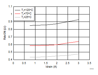
| Rds(ON) | FET ON resistance at 0.8 A for OD_x | TJ = 25°C | 0.35 | Ω | |||
| TJ = 120°C | 0.50 | ||||||
| 5 V-Low | 5.5-V VO at VDIN = VthV_ | VDIN = VthV_, VthV_ = 5-V load (dc) = 0.5 A(4) |
4 | V | |||
| VO voltage to 5.5 V | –30% | ||||||
| VO voltage drop from VDIN | 1 | V | |||||
| Vo_min6 | VO setting without kick UVP when VDIN = VthVM+ (VO setting at VDIN = 10 V) |
VthVM+ = 6-V load (DC) = 0.5 A(3) | 6 | V | |||
| THREE DC-DC CONVERTER PROTECTION | |||||||
| IO DD ODx | Overcurrent detect for OD_x source | Peak current in each ON cycle | 1.8 | 3 | A | ||
| tFILTOCP | OCP filtering time | By OSCi cycles | 2 | cycles | |||
| tODSD | DC-DC shutdown filter | Number of subsequent chopping cycles with OCP detection | 4 | chop cycles | |||
| Vovpx | Overvoltage protection (OVP) | Percentage of nominal Voutx detected at VFB | 25% | 30% | 35% | ||
| Vuvpx | Undervoltage protection (UVP) | Percentage of nominal Voutx detected at VFB (VFB decreasing) | -25% | -30% | -35% | ||
| tVfilter | OVP/UVP filtering time | 3 | 8 | 13 | us | ||
| tsst | Start-up time with soft start | 56 | ms | ||||
| Vstover | Start-up overshoot | Ratio to VO | 3% | ||||
| VM SUPERVISORY | |||||||
| VthVM– | nORT for VM low threshold | VM decreasing | 4.5 | 5 | 6 | V | |
| VthVM+ | nORT for VM high threshold | VM increasing | 5.5 | 6 | 7 | V | |
| VthVMh | nORT for VM detect hysteresis | (VthVM+) - (VthV—) | 0.5 | 1 | V | ||
| VthVM2 | For motor driver off (5) | 15 | V | ||||
| tVM filt | VM monitor filtering time | For VM threshold detect | 10 | 30 | μs | ||
| THERMAL SHUTDOWN (TSD) | |||||||
| TTSD | Thermal shutdown set points | 150 | 170 | 190 | °C | ||
| TEMPERATURE SENSE, PRE TSD (See Extended Setup Register Definition) | |||||||
| TTSD0 | Temperature sense point 0 | Register selectable, Assert logic H at TH_OUT |
130 | 150 | 170 | °C | |
| TTSD1 | Temperature sense point 1 | Register selectable, Assert logic H at TH_OUT |
120 | 140 | 160 | °C | |
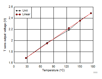
| Tc_sens | TH_OUT (analog out) temperature coefficient | Specified by design | 6 | mV/°C | |||
| RESET/NORT: OPEN-DRAIN OUTPUTS (NORT, LOGIC_OUT, TH_OUT) | |||||||
| VOH | High-state voltage | RL = 1 kΩ to 3.3 V | 3 | V | |||
| VOL | Low-state voltage | RL = 1 kΩ to 3.3 V | 0.3 | V | |||
| IOL | Low-state sink current | VO = 0.4 V | 3 | mA | |||
| tr | Rise time | 10% to 90% | 1 | μs | |||
| tf | Fall time | 90% to 10% | 50 | ns | |||
| RESET/NORT DELAY: START-UP SEQUENCE | |||||||
| tord1 | nORT delay 1 | Reset deassertion from VthVM+ < VDIN for DC-DC wake up falling | 300 | 390 | ms | ||
| tord3 | DC-DC turnon delay | From one DC-DC wake up to following DC-DC to go soft-start sequence | 1.7 | ms | |||
| tord4 | nORT delay 4 | Reset deassertion from 2nd DC-DC wake up | 120 | 180 | ms | ||
| In-Reset | |||||||
| treset | In-Reset assertion to nORT assertion delay | In-Reset falling to nORT failing | 5 | 10 | μs | ||
| H-BRIDGE DRIVERS (OUTX+ AND OUTX–) | |||||||
| IOUT1(max) | Peak output current 1 | Less than 500-ns period | 8 | A | |||
| IOUT2(max) | Peak output current 2 | Less than 100-ms period | 3 | A | |||
| IOUT(max) | Average continuous output current | 0.8 | A | ||||
| Rds(ON) | FET ON resistance at 0.8 A | TJ = 25°C | 0.55 | Ω | |||
| TJ = 120°C | 1 | ||||||
| ICEX | Output leakage current | VOUTX = 0 V or 10 V | 10 | μA | |||
| IRS | Sense resistor supply current | nORT = Low | 15 | μA | |||
| IOC Motor | Motor overcurrent threshold for each H-bridge(6) | 3 | 5 | A | |||
| tfilterM | Motor overcurrent filter time | 2.5 | 5 | 8.5 | μs | ||
| fOSCM | Motor oscillator frequency | F_OSCM = (0,0) | 720 | 800 | 880 | kHz | |
| fchop | Motor chopping frequency = fOSCM/8 |
F_OSCM = (0,0) | 90 | 100 | 110 | kHz | |
| STEPPER MOTOR DRIVE (PARAMETERS ARE TESTED WITHOUT MOTOR LOADING) | |||||||
| ISTEPMOTORAVG | Average stepper motor current for H-bridge |
VM = 40 V | 800 | mA | |||
| ISTEPMOTORPeak | Peak stepper motor current for H-bridge |
VM = 40 V | 1.3 | A | |||
| Stepper motor current limit threshold (internal reference)(7) |
VL16 , Phase angle = 90° | 100% | |||||
| VL15 , Phase angle = 84° | 100% | ||||||
| VL14 , Phase angle = 79° | 98% | ||||||
| VL13 , Phase angle = 73° | 96% | ||||||
| VL12 , Phase angle = 68° | 92% | ||||||
| VL11 , Phase angle = 62° | 88% | ||||||
| VL10 , Phase angle = 56° | 83% | ||||||
| VL9 , Phase angle = 51° | 77% | ||||||
| VL8 , Phase angle = 45° | 71% | ||||||
| VL7 , Phase angle = 40° | 63% | ||||||
| VL6 , Phase angle = 34° | 56% | ||||||
| VL5 , Phase angle = 28° | 47% | ||||||
| VL4 , Phase angle = 23° | 38% | ||||||
| VL3 , Phase angle = 17° | 29% | ||||||
| VL2 , Phase angle = 11° | 20% | ||||||
| VL1 , Phase angle = 6° | 10% | ||||||
| VL0 , Phase angle = 0° | 0% | ||||||
| IOUT | Output current accuracy at 100% setting(7) | Excludes VREF and RSENS errors, IOUT > 1 A(7)(8) |
–5% | 5% | |||
| IswLeakage | Switch (driver MOSFET) leakage current | Outputs off | –10 | 10 | μA | ||
| tab | Stepper motor blanking time | By OSCi cycles | 8 | 9 | cycles | ||
| STEPPER AND DC MOTOR DRIVERS | |||||||
| tr | Rise time | VM = 27 V | 100 | 300 | ns | ||
| tf | Fall time | 20% to 80% | 100 | 300 | ns | ||
| tPDOFF | Enable or strobe detection to sink or source gate off delay | 50 | 150 | 400 | ns | ||
| tCOD | Crossover delay time, to prevent shoot through | 100 | 600 | 1000 | ns | ||
| tPDON | Enable or strobe detection to sink or source gate on delay | 750 | ns | ||||
| DC MOTOR DRIVERS | |||||||
| tblank | Blanking time | TBLNK = (0,0) for Min, (1,1) for Max, fCHOP = 100 kHz |
1.6 | 5.65 | μs | ||
| twPminp | Minimum pulse duration (phase) | 1 | μs | ||||
| twPmine | Minimum pulse duration (enable) | 1 | μs | ||||
| SERIAL INTERFACE | |||||||
| f(CLK) | Clock frequency | 1 | 25 | MHz | |||
| twh(CLK) | Minimum high-level pulse width | 10 | ns | ||||
| twl(CLK) | Minimum low-level pulse width | 10 | ns | ||||
| tsu | Setup time, data to CLK↓ | 10 | ns | ||||
| th | Hold time, CLK↓ to data | 10 | ns | ||||
| tcs | CLK↓ to STROBE↑ | 10 | ns | ||||
| tsc | STROBE↓ to CLK↑ | 10 | ns | ||||
| tw(STRB) | Minimum strobe pulse duration | 20 | ns | ||||
| tss_min | Strobe mask time from nSLEEP | 1.5 | 4 | μs | |||
| SERIAL INTERFACE: ID MONITOR FUNCTION AT LOGIC_OUT, EXTENDED SETUP MODE | |||||||
| tODL | 0 data output delay bit 3 to bit 0 (ext-setup) = (1100) |
From strobe rise to LOGIC_OUT, 1 kΩ to external 3.3 V |
4000 | ns | |||
| tODH | 1 data output delay bit 3 to bit 0 (ext-setup) = (1111) |
From strobe rise to LOGIC_OUT, 1 kΩ to external 3.3 V |
4000 | ns | |||
(1) Absolute maximum rating for charge-pump circuit is 60 V.
(2) DCDC_MODE = H, Ch-B and Ch-C are in parallel driving mode.
(3) VOUT (at VDIN = VthVM+) is lower than VO setting. When VDIN is down to VthVM+, undervoltage protection (UVP) shuts down the device, in case the VO is set as VO > 7 V. Specified by design.
(4) Lower VDIN decrease gate drive and the voltage drop is increased. Specified by bench characterization only.
(5) No nORT assertion to VthVM2 detection
(6) When the overcurrent is detected, all H-bridges are shut down and assert nORT pulse (40 ms).
(7) This is not measured directly, checked by Itrip amplifier gain without motor loading
(8) This device may show current setting error when motor current is less than 1 A, due to noise filter delay at the Itrip comparator.
6.6 Typical Characteristics