SLVS854E July 2008 – December 2014 DRV8809
PRODUCTION DATA.
- 1 Features
- 2 Applications
- 3 Description
- 4 Revision History
- 5 Pin Configuration and Functions
- 6 Specifications
-
7 Detailed Description
- 7.1 Overview
- 7.2 Functional Block Diagram
- 7.3
Feature Description
- 7.3.1
Serial Interface
- 7.3.1.1 Setup Mode/Power-Down Mode
- 7.3.1.2 Extended Setup Mode
- 7.3.1.3 Serial Interface Timing
- 7.3.1.4 Bipolar Current Regulated Stepper Motor Drive
- 7.3.1.5 Short/Open for Motor Outputs
- 7.3.1.6 DCDC_MODE for Parallel-Mode Control
- 7.3.1.7 DCDC_MODE and C_SELECT Timing Delay and Start-Up Order
- 7.3.1.8 In-Reset: Input for System Reset
- 7.3.1.9 Blanking Time Insertion Timing for DC Motor Driving
- 7.3.2 Motor Driver Configuration
- 7.3.3 Charge Pump
- 7.3.1
Serial Interface
- 7.4 Device Functional Modes
- 7.5 Register Maps
- 8 Application and Implementation
- 9 Power Supply Recommendations
- 10Layout
- 11Device and Documentation Support
- 12Mechanical, Packaging, and Orderable Information
5 Pin Configuration and Functions
PAP Package
64 Pins
Top View
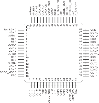
Pin Functions
| PIN | I/O | PULLUP/ PULLDOWN | SHUNT RESISTOR | DESCRIPTION | ||
|---|---|---|---|---|---|---|
| NO. | NAME IN SETUP MODE | NAME IN OPERATION | ||||
| 1 | Test-LGND | Test-LGND | - | Low power or analog ground | ||
| 2 | MGND | MGND | - | Power ground for motor | ||
| 3 | OUTA- | OUTA- | O | Motor-drive output for winding A– | ||
| 4 | RSA | RSA | I | Channel A current-sense resistor | ||
| 5 | RSA | RSA | I | Channel A current-sense resistor | ||
| 6 | OUTA+ | OUTA+ | O | Motor-drive output for winding A+ | ||
| 7 | MGND | MGND | - | Power ground for motor | ||
| 8 | MGND | MGND | - | Power ground for motor | ||
| 9 | OUTB+ | OUTB+ | O | Motor-drive output for winding B+ | ||
| 10 | RSB | RSB | I | Channel B current-sense resistor | ||
| 11 | RSB | RSB | I | Channel B current-sense resistor | ||
| 12 | OUTB- | OUTB- | O | Motor-drive output for winding B– | ||
| 13 | MGND | MGND | - | Power ground for motor | ||
| 14 | LGND | LGND | - | Low-power or analog ground | ||
| 15 | DCDC_MODE | DCDC_MODE | I | Up | 200 kΩ | DC-DC Ch-B/Ch-C operation mode select |
| 16 | FBC | FBC | I | Feedback signal for DC-DC converter C | ||
| 17 | OD_C | OD_C | O | Output for DC-DC switch mode regulator C | ||
| 18 | OD_C | OD_C | O | Output for DC-DC switch mode regulator C | ||
| 19 | OD_B | OD_B | O | Output for DC-DC switch mode regulator B | ||
| 20 | OD_B | OD_B | O | Output for DC-DC switch mode regulator B | ||
| 21 | FBB | FBB | I | Feedback signal for DC-DC converter B | ||
| 22 | VCP | VCP | - | Charge pump capacitor | ||
| 23 | OSCD_mon | OSCD_mon | O | OSCD clock monitoring | ||
| 24 | CP2 | CP2 | - | Charge-pump bucket capacitor (high side) | ||
| 25 | CP1 | CP1 | - | Charge-pump bucket capacitor (low side) | ||
| 26 | VDIN | VDIN | Voltage supply for DC-DC converter | |||
| 27 | VDIN | VDIN | Voltage supply for DC-DC converter | |||
| 28 | VDIN | VDIN | Voltage supply for DC-DC converter | |||
| 29 | VM | VM | - | Voltage supply for motors | ||
| 30 | VREF_AB | VREF_AB | I | Voltage reference for maximum stepper motor current through A and B bridges | ||
| 31 | VREF_CD | VREF_CD | I | Voltage reference for maximum stepper motor current through C and D bridges | ||
| 32 | FBA | FBA | I | Feedback signal for DC-DC converter A | ||
| 33 | OD_A | OD_A | O | Output for DC-DC switch mode regulator A | ||
| 34 | OD_A | OD_A | O | Output for DC-DC switch mode regulator A | ||
| 35 | LGND | LGND | - | Low-power or analog ground | ||
| 36 | MGND | MGND | - | Power ground for motor | ||
| 37 | OUTC– | OUTC– | O | Motor-drive output for winding C– | ||
| 38 | RSC | RSC | I | Channel C current-sense resistor | ||
| 39 | RSC | RSC | I | Channel C current-sense resistor | ||
| 40 | OUTC+ | OUTC+ | O | Motor-drive output for winding C+ | ||
| 41 | MGND | MGND | - | Power ground for motor | ||
| 42 | MGND | MGND | - | Power ground for motor | ||
| 43 | OUTD+ | OUTD+ | O | Motor-drive output for winding D+ | ||
| 44 | RSD | RSD | I | Channel D current-sense resistor | ||
| 45 | RSD | RSD | I | Channel D current-sense resistor | ||
| 46 | OUTD– | OUTD– | O | Motor drive output for winding D– | ||
| 47 | MGND | MGND | - | Power ground for motor | ||
| 48 | GND | GND | - | Must be grounded | ||
| 49 | C_SELECT | C_SELECT | I | Up | 200 kΩ | DC-DC converter selector |
| 50 | - | ENABLE_SD | I | Down | 100 kΩ | Enable input for DC motor D control |
| 50 | - | Reserved | I | Down | 100 kΩ | Reserved for DC motor operation |
| 51 | STROBE_CD | ENABLE_SC | I | Down | 100 kΩ | Enable for DC motor C control |
| 51 | STROBE_CD | ENABLE_LCD | I | Down | 100 kΩ | Enable for large DC motor CD control |
| 51 | STROBE_CD | STROBE_CD | I | Down | 100 kΩ | Serial interface data strobe for H-bridge C, D stepper motor drive (latch on rising edge) |
| 52 | TH_OUT | TH_OUT | O | Open drain | Temperature-sensing output | |
| 53 | LOGIC OUT | LOGIC OUT | O | Open drain | Protection-monitoring output | |
| 54 | - | Reserved | I | Down | 100 kΩ | Reserved for four DC motor operation |
| 54 | - | ENABLE_SB | I | Down | 100 kΩ | Enable for DC motor B control |
| 55 | STROBE_ AB | STROBE_ AB | I | Down | 100 kΩ | Serial interface data strobe for H-bridge A, B stepper motor drive (latch on rising edge) |
| 55 | STROBE_AB | ENABLE_LAB | I | Down | 100 kΩ | Enable for large DC motor AB control |
| 55 | STROBE_AB | ENABLE_SA | I | Down | 100 kΩ | Enable for DC motor A control |
| 56 | nORT | nORT | O | Open drain | Reset output (open drain) | |
| 57 | LGND | LGND | - | Low power or analog ground | ||
| 58 | OSCM_mon | OSCM_mon | O | Open drain | OSCM clock monitoring | |
| 59 | DATA_CD | PHASE_SD | I | Down | 100 kΩ | Serial input data for H-bridge C and D control |
| 59 | DATA_CD | DATA_CD | I | Down | 100 kΩ | Serial input data for H-bridge C and D control |
| 60 | CLK_CD | PHASE_SC | I | Down | 100 kΩ | Phase input for DC motor C control |
| 60 | CLK_CD | CLK_CD | I | Down | 100 kΩ | Clock input synchronization for serial data CD |
| 60 | CLK_CD | PHASE_LCD | I | Down | 100 kΩ | Phase input for large DC motor CD control |
| 61 | DATA_AB | DATA_AB | I | Down | 100 kΩ | Serial input data for H-bridge A and B control |
| 61 | DATA_AB | PHASE_SB | I | Down | 100 kΩ | Phase input for DC motor B control |
| 62 | CLK_AB | CLK_AB | I | Down | 100 kΩ | Clock input synchronization for serial data AB |
| 62 | CLK_AB | PHASE_LAB | I | Down | 100 kΩ | Phase input for large DC motor AB control |
| 62 | CLK_AB | PHASE_SA | I | Down | 100 kΩ | Phase input for DC motor A control |
| 63 | nSLEEP=L | nSLEEP | I | Down | 100 kΩ | Enable/disable (part can be in sleep state) |
| 64 | In-Reset | In-Reset | I | Up | 200 kΩ | Reset (L: Reset, H/open: Normal operation) |
Alternate Functions of Select Pins By Operation Mode
| CONFIG | PIN | |||||||
|---|---|---|---|---|---|---|---|---|
| 50 | 51 | 54 | 55 | 59 | 60 | 61 | 62 | |
| Default Name | ENABLE_SD | ENABLE_SC | ENABLE_SB | STROBE_AB | PHASE_ SD | PHASE_SC | DATA_AB | CLK_AB |
| Dual Stepper | - | STROBE_CD | - | STROBE_AB | DATA_CD | CLK_CD | DATA_AB | CLK_AB |
| Stepper + Large DC | - | ENABLE_LCD | - | STROBE_AB | - | PHASE_LCD | DATA_AB | CLK_AB |
| Stepper + Dual Small DC | ENABLE_SD | ENABLE_SC | - | STROBE_AB | PHASE_SD | PHASE_SC | DATA_AB | CLK_AB |
| Large DC + Dual Small DC | ENABLE_SD | ENABLE_SC | - | ENABLE_LAB | PHASE _SD | PHASE_SC | - | PHASE_LAB |
| Dual Large DC | - | ENABLE_LCD | - | ENABLE_LAB | - | PHASE_LCD | - | PHASE_LAB |
| Quad Small DC | ENABLE_SD | ENABLE_SC | ENABLE_SB | ENABLE_SA | PHASE_SD | PHASE_SC | PHASE_SB | PHASE_SA |
| Large Stepper | - | STROBE_CD | - | STROBE_AB | DATA_CD | CLK_CD | DATA_AB | CLK_AB |
| Ultra-Large DC | - | - | - | ENABLE_UL | - | - | - | PHASE_UL |
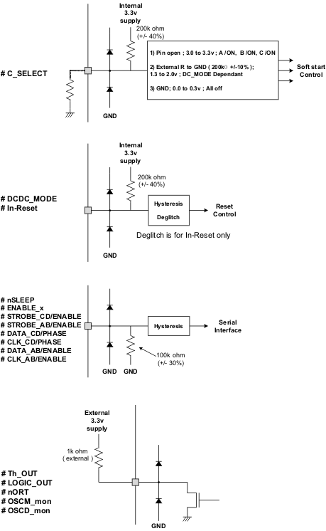 Figure 1. Input Pin Configurations
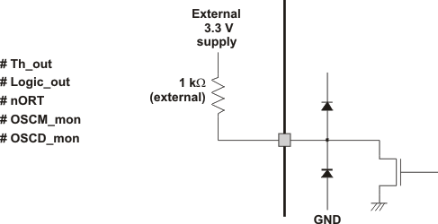 Figure 2. Open-Drain Output Pin Configurations