SLVS854E July 2008 – December 2014 DRV8809
PRODUCTION DATA.
- 1 Features
- 2 Applications
- 3 Description
- 4 Revision History
- 5 Pin Configuration and Functions
- 6 Specifications
-
7 Detailed Description
- 7.1 Overview
- 7.2 Functional Block Diagram
- 7.3
Feature Description
- 7.3.1
Serial Interface
- 7.3.1.1 Setup Mode/Power-Down Mode
- 7.3.1.2 Extended Setup Mode
- 7.3.1.3 Serial Interface Timing
- 7.3.1.4 Bipolar Current Regulated Stepper Motor Drive
- 7.3.1.5 Short/Open for Motor Outputs
- 7.3.1.6 DCDC_MODE for Parallel-Mode Control
- 7.3.1.7 DCDC_MODE and C_SELECT Timing Delay and Start-Up Order
- 7.3.1.8 In-Reset: Input for System Reset
- 7.3.1.9 Blanking Time Insertion Timing for DC Motor Driving
- 7.3.2 Motor Driver Configuration
- 7.3.3 Charge Pump
- 7.3.1
Serial Interface
- 7.4 Device Functional Modes
- 7.5 Register Maps
- 8 Application and Implementation
- 9 Power Supply Recommendations
- 10Layout
- 11Device and Documentation Support
- 12Mechanical, Packaging, and Orderable Information
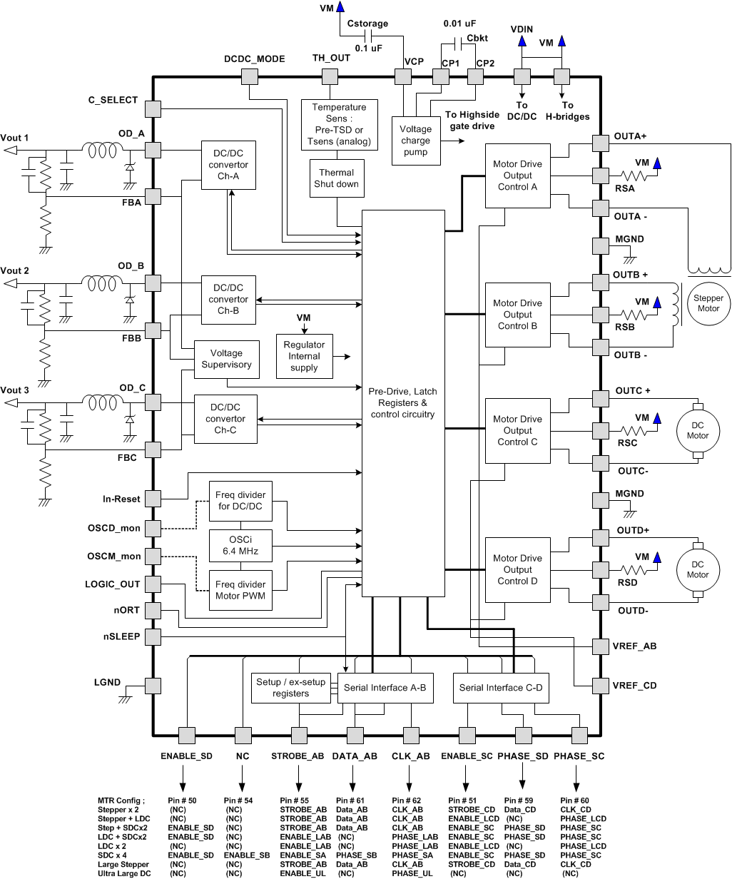
7 Detailed Description
7.1 Overview
The DRV8809/DRV8810 provides an integrated motor driver solution. The chip has four H-bridges internally and is configurable to eight different modes of combination motor driver control. The output driver block for each H-bridge consists of N-channel power MOSFETs configured as full H-bridges to drive the motor windings. Their Rdson is low, 0.55 ohm at Tj = 25 C, it allows 800 mA maximum continuous current and 3 A @ 100 ms peak current. The stepper motor control has a 16-step mode programmable through the three-wire serial interface (SPI). The SPI input pins are 3.3-V compatible and 5-V tolerant. The DRV8809/DRV8810 has three DC-DC switch-mode buck converters to generate a programmable output voltage from 1.5 V to 80% of VDIN (Channel A) or up to 10 V (for Channel B and Channel C), with up to 1.5-A load current capability. Their Rdson is low, 0.35 ohm only at Tj = 25 C. The outputs are selected using the C_SELECT terminal at start-up or using serial interface during operation. An internal shutdown function is provided for overcurrent protection (OCP), short-circuit protection, overvoltage/undervoltage lockout (UVLO), and thermal shutdown (TSD). Also, the device has a reset function that operates at power on and at input to the In-Reset pin.
7.2 Functional Block Diagram
7.3 Feature Description
7.3.1 Serial Interface
The device has two serial interface circuit blocks for stepper motor driving control. These two serial interfaces provide controls to each motor driver independently.
| CLKAB | Serial clock for H-bridge A, B |
| DATAAB | Serial data for H-bridge A, B |
| STROBEAB | Strobe input for H-bridge A, B |
| CLKCD | Serial clock for H-bridge C, D |
| DATACD | Serial data for H-bridge C, D |
| STROBECD | Strobe signal for H-bridge C, D |
Sixteen bits serial data is shifted into the least significant bit (LSB) of the serial data input (DATA) shift register on the falling edge of the serial clock (CLK). After 16 bits of data transfer, the strobe signal (Strobe) rising edge latches all the shifted data. During data transfer, Strobe voltage level is acceptable high or low.
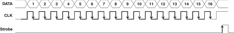 Figure 5. Serial Interface
7.3.1.1 Setup Mode/Power-Down Mode
The motor output mode is configured through serial interface (DATA AB, CLK AB and STROBEAB) when nSLEEP = L. After setup, the nSLEEP pin must be pulled high for normal motor drive control. The condition that the device requires for setup (initialization) is after the nORT (Reset) output goes to high from the low level (power on, recovery from VM < 7 V). While nSLEEP is low, all the motor drive functions are shut down and their outputs are high-impedance state. Also the stepper parameters in the register are all reset to 0. This device forces motor driver functions to shut down for the power-down mode, and it is not damaged even if nSLEEP is asserted during motor driving. At the Strobe pulse rising edge, the DATA signal level must be low for normal setup mode (see the Extended Setup Mode section for another option).
7.3.1.2 Extended Setup Mode
While nSLEEP = L, if the DATA signal level is set high when the Strobe pulse is set, the serial interface recognizes the input data to set the extended setup mode. This extended setup register enables monitoring and controlling the fault condition of this chip. One of the internal protection control signals is selected and provided to LOGIC OUT pin. Also, this enables the application to ignore the protection control and/or suppress the reset signal generation. This device has device ID (3-bit ROM) and vendor ID (1-bit ROM), which can be read out from LOGIC OUT. Four bits are assigned to select the LOGIC OUT signal, including the ID ROM bit readout.
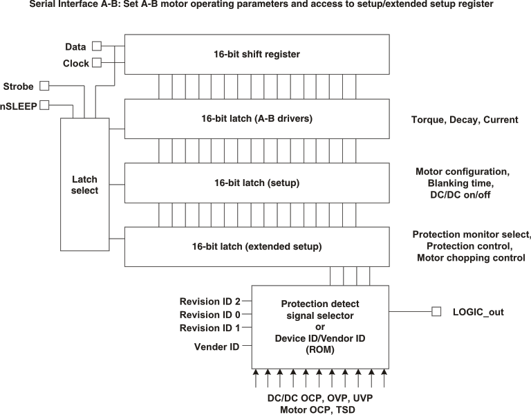
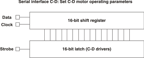 Figure 7. Serial Interface C-D
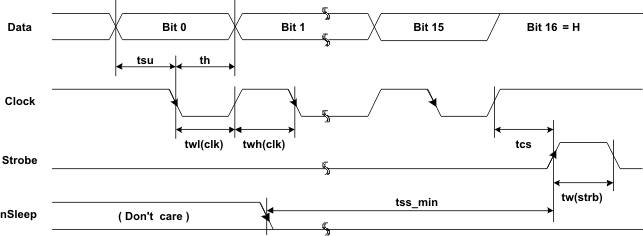
7.3.1.3 Serial Interface Timing
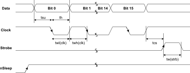 Figure 8. nSLEEP = H: Set Stepper Motor Operating Parameters
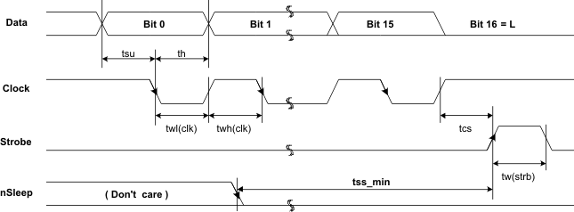 Figure 9. nSLEEP = L (Bit 16 = L): Setup Mode
7.3.1.4 Bipolar Current Regulated Stepper Motor Drive
The following functionality is common to all the H-bridge drives. A crossover delay is inherent to the control circuitry to prevent cross conduction of the upper and lower switches on the same side of the H-bridge. A blanking (deglitch) time is incorporated to prevent false triggering due to initial current spikes at turnon with a discharged capacitive load.
The stepper motor current can be programmed to 16 different current levels using a 4-bit register. The average current level for a particular angular rotation is shown in Table 1.
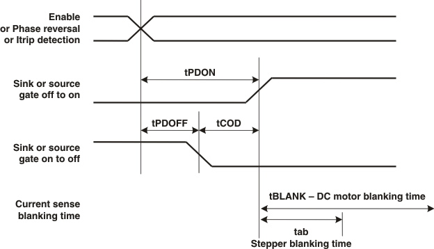 Figure 11. Crossover and Blanking Timing for H-Bridge
For stepper motor configured H-bridges, only tab (stepper blanking time) is set for current sensing. For DC motor-configured H-bridges, tBLANK is included to ignore huge current spike due to rush current to varistor capacitance.
7.3.1.5 Short/Open for Motor Outputs
When a short/open situation happens, the protection circuit prevents device damage under certain conditions (short at start up, and so forth).
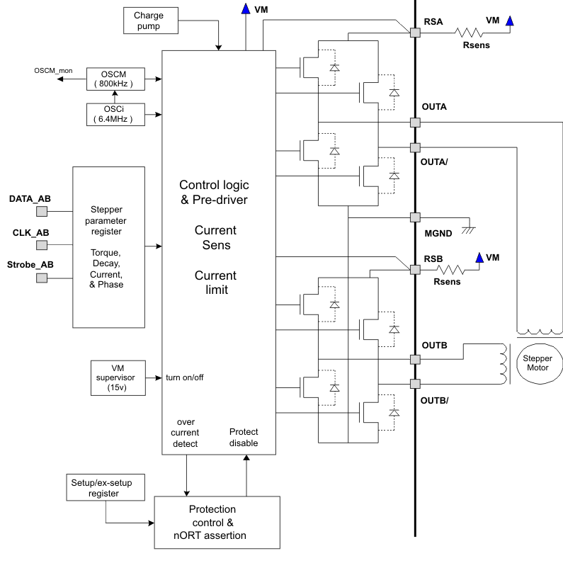 Figure 12. Stepper Motor Driver
Table 1. Angular Rotation Setting for Stepping Motor Driver (Parameter Bit in Stepper Register)
| STEP | SET ANGLE (deg) |
BIT 14 | BIT 13 | BIT 12 | BIT 11 | BIT 7 | BIT 6 | BIT 5 | BIT 4 |
|---|---|---|---|---|---|---|---|---|---|
| CURRENT A (C) 3 |
CURRENT A (C) 2 |
CURRENT A (C) 1 |
CURRENT A (C) 0 |
CURRENT B (D) 3 |
CURRENT B (D) 2 |
CURRENT B (D) 1 |
CURRENT B (D) 0 |
||
| 16 | 90 | H | H | H | H | L | L | L | L |
| 15 | 84.4 | H | H | H | H | L | L | L | H |
| 14 | 78.8 | H | H | H | L | L | L | H | L |
| 13 | 73.1 | H | H | L | H | L | L | H | H |
| 12 | 67.5 | H | H | L | L | L | H | L | L |
| 11 | 61.2 | H | L | H | H | L | H | L | H |
| 10 | 56.3 | H | L | H | L | L | H | H | L |
| 9 | 50.6 | H | L | L | H | L | H | H | H |
| 8 | 45 | H | L | L | L | H | L | L | L |
| 7 | 39.4 | L | H | H | H | H | L | L | H |
| 6 | 33.8 | L | H | H | L | H | L | H | L |
| 5 | 28.1 | L | H | L | H | H | L | H | H |
| 4 | 22.5 | L | H | L | L | H | H | L | L |
| 3 | 16.9 | L | L | H | H | H | H | L | H |
| 2 | 11.3 | L | L | H | L | H | H | H | L |
| 1 | 5.6 | L | L | L | H | H | H | H | H |
| 0 | 0 | L | L | L | L | H | H | H | H |
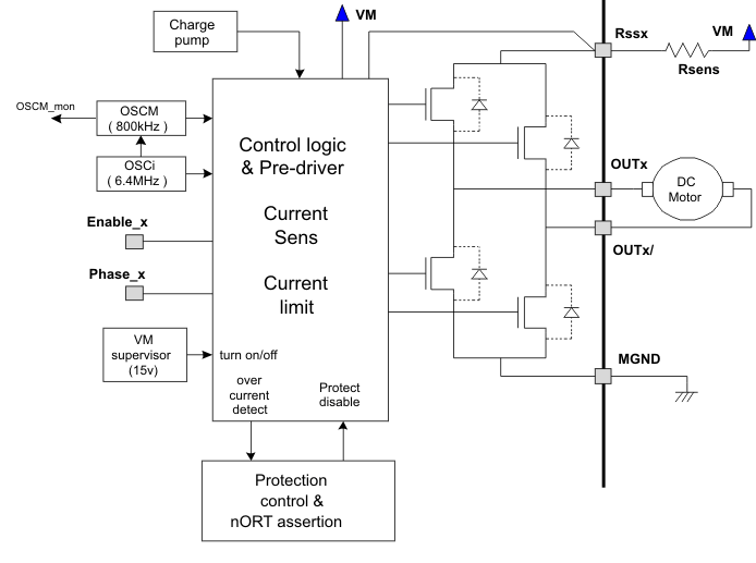 Figure 14. DC Motor Drive
The motor configuration setup bits in the setup register can select three types of DC motor driving: utilizing a single H-bridge, utilizing two (A and B, or C and D) H-bridges in parallel, or utilizing four H-bridges in parallel.
For the setup register value (bit 2,1,0) = (1,0,1), the device configuration is 4× DC motor, which enables each H-bridge to drive a DC motor independently. The ENABLEx and PHASEx input terminals are reassigned from the serial interface pins and some reserved pins, after nSLEEP pin is set to H.
For the setup register value (bit 2,1,0) = (0,1,1), the device configuration is 1× large DC + 2× DC motor mode. The large DC driving utilizes two H-bridges in parallel and controlled by ENABLE_AB and PHASE_AB pins. Two Rsens pins should be connected together.
The VREF inputs are used for the Rsense comparator reference voltage. VREF_AB provides the voltage to both H-bridge A and B, and VREF_CD provides the voltage for H-bridge C and D.
Table 2. DC Motor Drive Truth Table
| FAULT CONDITION | nSLEEP | ENABLEX | PHASEX | + HIGH SIDE | + LOW SIDE | - HIGH SIDE | - LOW SIDE |
|---|---|---|---|---|---|---|---|
| 0 | 0 | X | X | OFF | OFF | OFF | OFF |
| 0 | 1 | 0 | X | OFF | OFF | OFF | OFF |
| 0 | 1 | 1 | 0 | OFF | ON | ON | OFF |
| 0 | 1 | 1 | 1 | ON | OFF | OFF | ON |
| Motor OCP | 1 | X | X | OFF | OFF | OFF | OFF |
| TSD | X | X | X | OFF | OFF | OFF | OFF |
7.3.1.6 DCDC_MODE for Parallel-Mode Control
The DCDC_MODE pin selects the DC-DC converter parallel driving for Ch-B and Ch-C. The input is pulled up to internal 3.3 V by a 200-kΩ resistor. When the pin is H or left open, Ch-B and Ch-C are driven in parallel.
Table 3. C_SELECT for Start-Up
| C_SELECT | PIN VOLTAGE | DC-DC Vout1, ODA |
DC-DC Vout2, ODB |
DC-DC Vout3, ODC |
|---|---|---|---|---|
| Gnd | 0 V to 0.3 V | OFF | OFF | OFF |
| Pull Down (by external 200 kW) |
1.3 V to 2 V | See Table 4 | ||
| OPEN | 3 V to 3.3 V | ON | ON | ON |
7.3.1.7 DCDC_MODE and C_SELECT Timing Delay and Start-Up Order
DCDC_MODE and C_SELECT play a role in the order of regulator enablement, as well as the time when the first regulator is enabled to when the second is enabled. Regulators B and C are always enabled together, whether they are working in parallel mode or not.
Table 4. DCDC_MODE and C_SELECT Timing Delay (DRV8809)
| DCDC_MODE | C_SELECT | TIMING DELAY | DESCRIPTION |
|---|---|---|---|
| L | GND | None | No regulator is enabled. |
| L | Pull down | None | No regulator is enabled. |
| L | 3 V to 3.3 V | 1.6 ms | Ch-A followed by Ch-B and Ch-C |
| H | GND | None | No regulator is enabled. |
| H | Pull down | 1.6 ms | Ch-B and Ch-C followed by Ch-A |
| H | 3 V to 3.3 V | 1.6 ms | Ch-A followed by Ch-B and Ch-C |
Table 5. DCDC_MODE and C_SELECT Timing Delay (DRV8810)
| DCDC_MODE | C_SELECT | TIMING DELAY | DESCRIPTION |
|---|---|---|---|
| L | GND | None | No regulator is enabled. |
| L | Pull down | None | No regulator is enabled. |
| L | 3 V to 3.3 V | 1.6 ms | Ch-A followed by Ch-B and Ch-C |
| H | GND | None | No regulator is enabled. |
| H | Pull down | 20 ms to 40 ms | Ch-B and Ch-C followed by Ch-A |
| H | 3 V to 3.3 V | 20 ms to 40 ms | Ch-A followed by Ch-B and Ch-C |
7.3.1.8 In-Reset: Input for System Reset
In-Reset pin assertion stops all the DC-DC converters and H-bridges. It also reset all the register contents to default value. After deassertion of the input, the device follows the initial start-up sequence. The C_SELECT state is captured after the In-Reset deassertion. The input is pulled up to internal 3.3 V by 200-kΩ resistor. When the pin = H or left open, reset function is asserted. Also it has deglitch filter of 2.5 μs to 7.5 μs.
NOTE
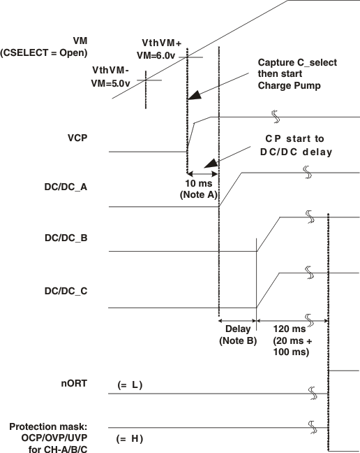
When VM crosses VthVM+ (about 6 V), the C_select state is captured. If C_SELECT is open (pulled up to internal 3.3 V), all DC-DC regulator channels (A, B, and C) are turned on. The time of channels B and C to be turned on, with regards to channel A, depends on the state of DC_MODE.
 Figure 16. Power-Up Timing (Power Up Without DC-DC Turn-On: C_SELECT = GND)
NOTE
When VM crosses VthVM+ (about 6 V) with C_SELECT = GND, none of the three regulators are turned on. The nORT output is released to H after 300 ms from the VthVM+ crossing.
NOTE
The regulator is started from the strobe input, same as charge pump. There is no 10-ms waiting period, because VCP pin already reached VM – 0.7 V.
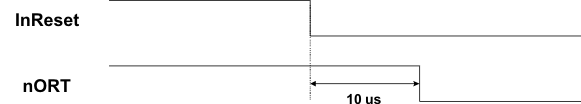 Figure 24. Shutdown by In-Reset
7.3.1.9 Blanking Time Insertion Timing for DC Motor Driving
For the DC motor driving H-bridge, tBlank is inserted at each phase reversal and also following each chopping cycle (once every eight OSCM clocks).
For a large n number (5 or 6) tBlank setup may decrease the itrip detect window. The user must be careful to optimize in the system.
Case A: Phase duty = 25%
Case A*1 for setup bit = (1,0)
Case A*2 for setup bit = (0,1)
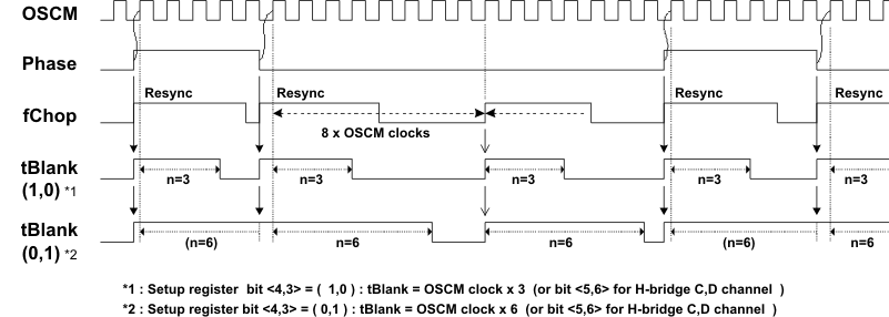 Figure 25. Blanking Time Insertion Timing, Case A
Case B: Phase duty = 40%
Case B*1 for setup bit =(1,0)
Case B*2 for setup bit =(0,1)
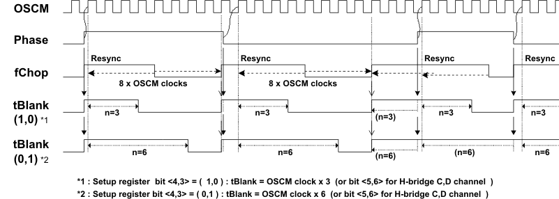 Figure 26. Blanking Time Insertion Timing, Case B
Table 6. Function Table nORT, Power Down, VM < 4.5 V Conditions
| DEVICE STATUS | CHARGE PUMP | OSCD | OSCM | nORT (RESET) OUTPUT | MODE SETTING |
|---|---|---|---|---|---|
| nSLEEP | Active | Active | Active | Inactive | Available |
| nORT | Inactive | Active | Active | Active | Depend on power down |
| VM < 6 V during power down | Active | Active | Active | See timing chart | Depend on power down |
| 4.5 V < VM | Inactive | Inactive | Inactive | Active | Unavailable |
Table 7. Shutdown Functions
| CASE OF SUPPLY SHUTDOWN | DC-DC Vout1 | DC-DC Vout2 | DC-DC Vout3 | MOTOR | nORT (RESET) |
|---|---|---|---|---|---|
| DC-DC Vout1 OCP, OVP | Shut down | Shut down | Shut down | Shut down | Reset ON (L out) |
| DC-DC Vout2 OCP, OVP | Shut down | Shut down | Shut down | Shut down | Reset ON (L out) |
| DC-DC Vout3 OCP, OVP | Shut down | Shut down | Shut down | Shut down | Reset ON (L out) |
| Motor OCP | NA | NA | NA | OFF | Reset one pulse (tlow = 40 ms) |
| TSD | Shut down | Shut down | Shut down | Shut down | Reset ON (L out) |
- Shutdown of DC-DCs is released at VM > VthVM+ when VM is increasing. In case VM decreases, DC-DCs are shut down when VM <VthV_. When VM decreases and VthVM+ > VM > VthV_, the DC-DC output voltage supervisor is ignored.
- Motor shutdown is released by VM < 4.5 V or nSLEEP rising edge.
- nORT (reset) ON/OFF time is 40 ms.
- The data in Table 21 is valid if the protection control bits in the EX-setup register are all 0.
Table 8. Modes of Operation(1)(2)
| POR | M OFF | ISD | OVP | TSD | EXTERNAL PIN | IC | BLOCK FUNCTIONS | ||||||||||
|---|---|---|---|---|---|---|---|---|---|---|---|---|---|---|---|---|---|
| VM | VM | Vout1 | Vout2 | Vout3 | MOTOR | Vout1 | Vout2 | Vout3 | MOTOR | nSLEEP | CSEL | MOTOR | Vout1 | Vout2 | Vout3 | nORT | |
| 0 | 0 | 0 | 0 | 0 | 0 | 0 | 0 | 0 | 0 | H | N | On | On | On | On | H | |
| 1 | X | X | X | X | X | X | X | X | X | X | X | Off | Off | Off | Off | Off | L |
| 0 | 1 | X | X | X | X | X | X | X | X | X | X | O | On | Off | On/Off | On/Off | H |
| 0 | 1 | X | X | X | X | X | X | X | X | X | p | S/D | S/D | S/D | S/D | L | |
| 0 | 1 | X | X | X | X | X | X | X | X | e | S/D | S/D | S/D | S/D | L | ||
| 0 | 1 | X | X | X | X | X | X | X | r | S/D | S/D | S/D | S/D | L | |||
| 0 | 1 | X | X | X | X | X | X | a | Off | On | On | On | L/P | ||||
| 0 | 1 | X | X | X | X | X | t | S/D | S/D | S/D | S/D | L | |||||
| 0 | 1 | X | X | X | X | I | S/D | S/D | S/D | S/D | L | ||||||
| 0 | 1 | X | X | X | o | S/D | S/D | S/D | S/D | L | |||||||
| 0 | 1 | X | X | n | S/D | S/D | S/D | S/D | L | ||||||||
| 0 | Low | X | S | Off | On | On | On | H | |||||||||
| High | All off | X | Off | Off | Off | L | |||||||||||
| 200 k | X | On | On | Off | H | ||||||||||||
| Open | X | Off | On | On | H | ||||||||||||
7.3.2 Motor Driver Configuration
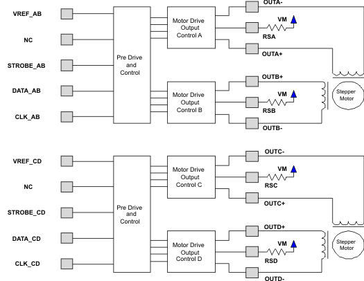 Figure 27. Motor Configuration 0, Two Stepper
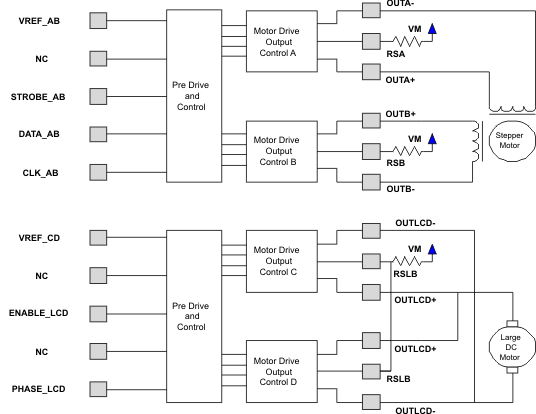 Figure 28. Motor Configuration 1, One Stepper and One Large DC
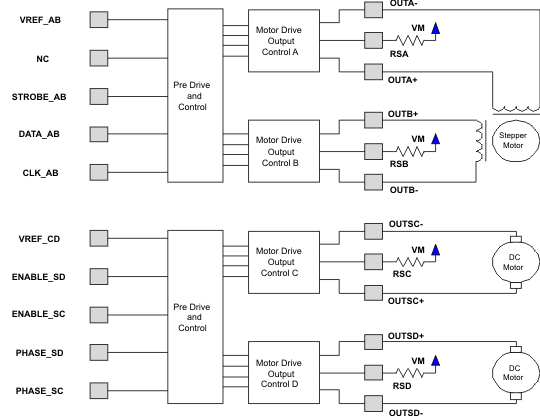 Figure 29. Motor Configuration 2, One Stepper and Two Small DCs
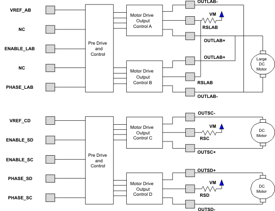 Figure 30. Motor Configuration 3, One Large DC and Two Small DCs
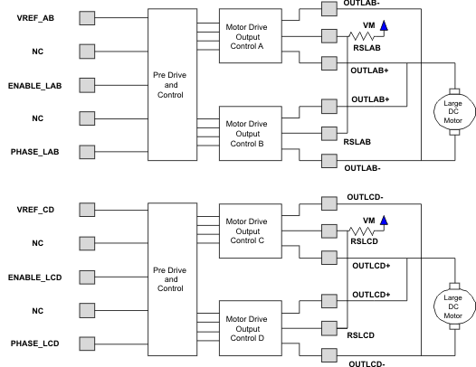 Figure 31. Motor Configuration 4, Two Large DCs
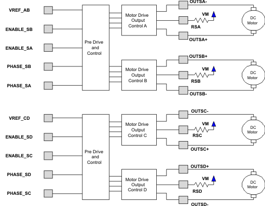 Figure 32. Motor Configuration 5, Four Small DCs
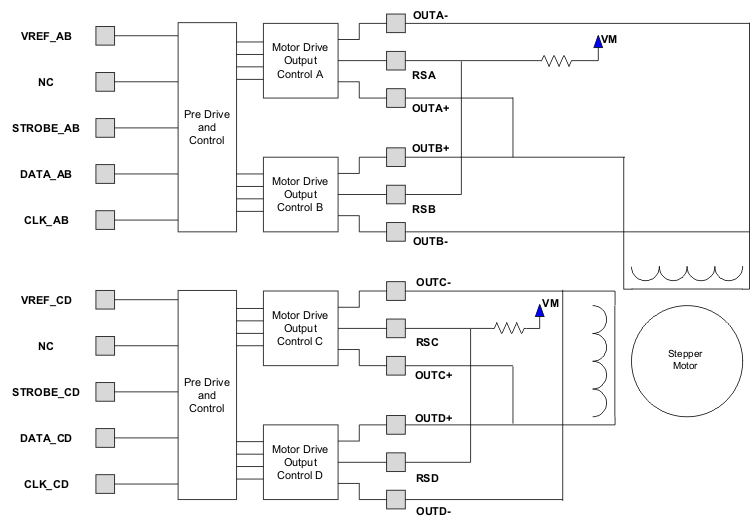 Figure 33. Motor Configuration 6, Single Large Stepper Motor
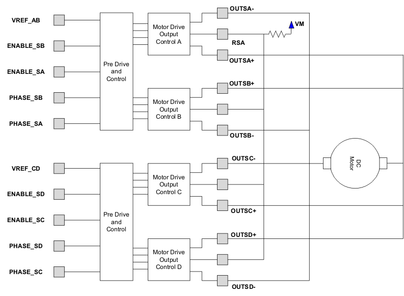 Figure 34. Motor Configuration 7, Ultra-Large DC
7.3.3 Charge Pump
The charge-pump voltage-generator circuit utilizes external storage and bucket capacitors. It provides the necessary voltage to drive the high-side switches for both DC-DC regulators and motor drivers. The charge-pump circuit is driven at a frequency of 1.6 MHz (nom). Recommended bucket capacitance is 10 nF, 16 V (min), and storage capacitance is 0.1 μF, 60 V (min). The charge-pump storage capacitor, Cstage, should be connected from the VCP output, pin 22, to VM.
For power-saving purposes in sleep mode, the charge pump is stopped when n_sleep = L and all three regulators are turned OFF. When the part is powered up, the charge pump is started first after the C_select capture, and 10 ms after the CP startup, the first regulator is started up.
Table 9. Charge Pump
| FAULT CONDITION | DC-DC Ch-A | DC-DC Ch-B | DC-DC Ch-C | nSLEEP | CHARGE PUMP |
|---|---|---|---|---|---|
| 0 | OFF | OFF | OFF | 0 | OFF |
| 0 | ON | X | X | X | ON |
| 0 | X | ON | X | X | ON |
| 0 | X | X | ON | X | ON |
| 0 | X | X | X | 1 | ON |
| Motor OCP | X | X | X | 1 | ON |
| TSD | X | X | X | X | OFF |
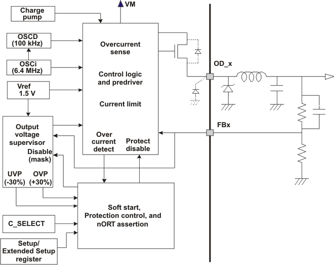 Figure 35. DC-DC Converter
This is a switch-mode regulator with integrated switches, to provide a programmed output set by the feedback terminal. The DC-DC converter has a fixed frequency variable duty cycle topology with a switching frequency of 100 kHz (nom). External filtering (inductor and capacitor) and external catch diode are required. The output voltage is short-circuit protected. If the system has a high input voltage and a very light load on the output, the converter may not provide energy to the inductor (skip) until the load line or the minimum voltage threshold is reached.
The regulator has a soft-start function to limit the rush current during start up. It is achieved by using VFB ramp during soft start.
For unused DC-DC converter channels, the external components can be removed if the channel is set to inactive by the C_SELECT pin and register bits. Also, the VFB pin can be left open or connected to ground.
DCDC_MODE selector can operate channel B and C in parallel mode to handle 2× output driving capability. VFB_B pin is active for feedback, and VFB_C pin must be pulled down internally.
7.4 Device Functional Modes
7.4.1 Operation With 7 V < VM and VDIN < 18 V
The devices starts operating with input voltages above 6.0 V typ. Between 7 V and 18 V, DC-DC converters can operate. Enabling motors in not allowed.
7.4.2 Operation With 18 V ≤ VM and VDIN ≤ 40 V
The device can operate with full function. Both DC-DC converter and motor drivers can be enabled.
7.5 Register Maps
7.5.1 Setup Register Bit Assignment
Setup register bits are assigned for motor configuration, blanking time, gain, and DC-DC switches. This register can be accessed only in Setup mode (nSLEEP = L and bit 16 data = L) .
Table 10. Setup Register
| BIT NO. | NAME | DEFAULT | DESCRIPTION |
|---|---|---|---|
| 0 | Motor select 0 | 0 | Motor configuration, < 2,1,0 > (0,0,0): Stepper × 2 (default) (0,0,1): Stepper + LDC, (0,1,0): Stepper + 2 × sDCs (0,1,1): DCL + 2 × sDC, (1,0,0): DCL × 2 (1,0,1): 4 × sDC (1,1,0): Large stepper (1,1,1): Ultra-large DC |
| 1 | Motor select 1 | 0 | |
| 2 | Motor select 2 | 0 | |
| 3 | TBLNK AB0 | 0 | Tblank for DC motor driving, Tblank is inserted at any phase change and beginning of each chopping cycle. AB1 AB0: Blanking time for A/B side drivers, CD1 CD0: Blanking time for C/D side drivers, 00: (1 ÷ fCHOP) ÷ 8 × 5 (= 6.25 μs) (default) 01: (1 ÷ fCHOP) ÷ 8 × 6 (= 7.50 μs) 10: (1 ÷ fCHOP) ÷ 8 × 3 (= 3.75 μs) 11: (1 ÷ fCHOP) ÷ 8 × 4 (= 5.00 μs) For stepper motor driving, only the fixed blanking time is applied. |
| 4 | TBLNK AB1 | 0 | |
| 5 | TBLNK CD0 | 0 | |
| 6 | TBLNK CD1 | 0 | |
| 7 | DC/DC_A SW | 0 | DC-DC ODA control, 0: ON (default), 1: OFF |
| 8 | DC/DC_B SW | 0 | DC-DC ODB control, 0: ON (default), 1: OFF |
| 9 | DC/DC_C SW | 0 | DC-DC ODC control, 0: ON (default), 1: OFF This bit is ignored when DCDC_MODE = H or open |
| 10 | Motor_AB gain | 0 | 0: 1/10 (default), 1: 0 |
| 11 | Motor_CD gain | 0 | 0: 1/10 (default), 1: 0 |
| 12 | OSCD frequency 0 | 0 | <1,0> = (0,0) 100 kHz (default) (0,1) 50 kHz (1,0) 200 kHz (1,1) 132.5 kHz These setup bits can be changed when the DC-DC regulators are in operation. |
| 13 | OSCD frequency 1 | 0 | |
| 14 | OSCM frequency 0 | 0 | <1,0> = (0,0) 800 kHz (default) (0,1) 400 kHz (1,0) 1.06 MHz (1,1) 1.6 MHz |
| 15 | OSCM frequency 1 | 0 |
The device can be configured to one out of eight different motor control combination modes. When the device is powered on or is recovering from reset, the mode can be selected by writing to the setup register through the serial interface AB, during Setup mode (nSLEEP = L).
Table 11. DC and Stepper Motor Configuration
| SETUP REGISTER | H-BRIDGE AND MOTOR CONFIGURATION | |||||
|---|---|---|---|---|---|---|
| BIT 2 | BIT 1 | BIT 0 | OUTA+, OUTA– | OUTB+, OUTB– | OUTC+, OUTC– | OUTD+, OUTD– |
| 0 | 0 | 0 | Stepper motor drive | Stepper motor drive | ||
| 0 | 0 | 1 | Stepper motor drive | Large DC motor drive | ||
| 0 | 1 | 0 | Stepper motor drive | DC motor drive | DC motor drive | |
| 0 | 1 | 1 | Large DC motor drive | DC motor drive | DC motor drive | |
| 1 | 0 | 0 | Large DC motor drive | Large DC motor drive | ||
| 1 | 0 | 1 | DC motor drive | DC motor drive | DC motor drive | DC motor drive |
| 1 | 1 | 0 | Large stepper motor drive: A + B for first winding, C + D for second winding | |||
| 1 | 1 | 1 | Ultra-large DC motor drive | |||
| Default setting is (M0, M1, M2) = (0, 0, 0) | ||||||
Extended setup (EX-setup) register bits are assigned for protection control, pre TSD, and multiplexer test mode selection. This register can be accessed only in Setup mode (nSLEEP = L and bit 16 data = H).
Table 12. Extended Setup Register (EX-Setup) Bit Assignment
| BIT NO. | NAME | DEFAULT | DESCRIPTION |
|---|---|---|---|
| 0 | Signal select 0 | 0 | Signal selector monitored on LOGIC_OUT DC-DC OCP detection, DC-DC voltage supervisor (OVP or UVP), Motor overcurrent (four H-bridges), TSD, and so forth [shutdown (protection) signals must be latched] |
| 1 | Signal select 1 | 0 | |
| 2 | Signal select 2 | 0 | |
| 3 | Signal select 3 | 0 | |
| 4 | Ignore SD 0 | 0 | 0 = Normal operation, 1 = Ignore DC-DC OCP |
| 5 | Ignore SD 1 | 0 | 0 = Normal operation, 1 = Ignore DC-DC voltage supervisor |
| 6 | Ignore SD 2 | 0 | 0 = Normal operation, 1 = Ignore motor OCP |
| 7 | Ignore SD 3 | 0 | 0 = Normal operation, 1 = Ignore thermal shutdown |
| 8 | Disable nORT 0 (selective shutdown for DC-DC Ch-C) |
0 | 0 = Normal operation 1 = Disable nORT assertion but shut down DC-DC Ch-C, in case of DC-DC Ch-C fault condition Ch-C shutdown is released by nSLEEP rise edge. If fault condition is on the other channels (with bit = 0), assert nORT and shut down all three DC-DC channels. This bit is ignored when DCDC_MODE = H or open |
| 9 | Disable nORT 1 (Selective shutdown for DC-DC Ch-B) |
0 | 0 = Normal operation 1 = Disable nORT assertion but shut down DC-DC channel B, in case of DC-DC Ch-B fault condition Ch-B shutdown is released by nSLEEP rise edge. If fault condition on the other channels (with bit = 0), assert nORT and shut down all three DC-DC channels. |
| 10 | Disable nORT 2 (Selective shutdown for DC-DC Ch-A) |
0 | 0 = Normal operation, 1 = Disable nORT assertion but shutdown the DC-DC Ch-A, in case of DC-DC Ch-A fault condition. Ch-A shutdown is released by nSLEEP rise edge. If fault condition on the other channels (with bit is 0), assert nORT and shut down all three DC-DC channels . |
| 11 | Pre TSD 0 | 0 | 0 = Ttsd0 = Ttsd - 20°C, 1 = Ttsd1= Ttsd - 30°C |
| 12 | Pre TSD 1 | 0 | 0 = Pre-TSD (logic) output, 1 = TH_OUT Analog output |
| 13 | Test mux 0 | 0 | Test mode selection, < 2,1,0 > = (0,0,0) Normal operation (0,0,1) TSD control – 1, (0,1,0) TSD control – 2, (0,1,1) OSC monitor enable, |
| 14 | Test mux 1 | 0 | |
| 15 | Test mux 2 | 0 |
Table 13. LOGIC OUT Selection
| NO. | EX-setup REGISTER (BITS 3–0) | SIGNAL SELECTION MONITORED ON LOGIC OUT (LISTED SIGNALS TO BE MUXED BY OR) |
SIGNAL POINT | ||
|---|---|---|---|---|---|
| 0 | 0000 (default) | DC-DC OCP_A | DC-DC OVP_A | DC-DC UVP_A | Latched out |
| 1 | 0001 | DC-DC OCP_B | DC-DC OVP_B | DC-DC UVP_B | Latched out |
| 2 | 0010 | DC-DC OCP_C | DC-DC OVP_C | DC-DC UVP_C | Latched out |
| This bit is ignored when DCDC_MODE pin = H or open. | |||||
| 3 | 0011 | DC-DC OCP_A | DC-DC OCP_B | DC-DC OCP_C | Latched out |
| 4 | 0100 | DC-DC OVP_A | DC-DC OVP_B | DC-DC OVP_C | Latched out |
| 5 | 0101 | DC-DC UVP_A | DC-DC UVP_B | DC-DC UVP_C | Latched out |
| 6 | 0110 | Motor OCP | Latched out | ||
| 7 | 0111 | TSD | Latched out | ||
| 8 | 1000 | Revision <0> = 1: For this device <2,1,0> = (1,0,1) = 5 | ROM | ||
| 9 | 1001 | Revision <1> = 0: For this device | ROM | ||
| 10 | 1010 | Revision <2> = 1: For this device | ROM | ||
| 11 | 1011 | Vendor <0> = 0: For TI <1,0> = TI (0,0), NG (1,0) | ROM | ||
| 12 | 1100 | Vendor <1> = 0: For TI <1,0> = Reserve (0,1), (1,1) | ROM | ||
| 13 | 1101 | Internal oscillator clock (as divided by 32 = 200 kHz) | |||
| 14 | 1110 | Fixed value as 1 (open-drain output buffer off) | |||
| 15 | 1111 | Fixed value as 1 (open-drain output buffer off) | |||
Table 14. Test Mux Selection
| NO. | BITS 15, 14, 13 | DESCRIPTION | |
|---|---|---|---|
| 0 | 0, 0, 0 | Normal operation | |
| 1 | 0, 0, 1 | TSD control 1 | At TSD event, shut down only motor driver part, DC-DC keep ON, keep setup register values, motor shutdown released by nSLEEP = L, no nORT assertion |
| 2 | 0, 1, 0 | TSD control 2 | At TSD event, shut down only motor driver part, DC-DC keep ON, keep setup register values, motor shutdown released by nSLEEP = L, nORT assertion: 40-ms single pulse |
| 3 | 0, 1, 1 | OSC monitor enable | Provide clock to OSCD_mon and OSCM_mon pins |
The serial interfaces communicate to the stepper parameter registers during nSLEEP = H . When nSLEEP = L, all register values are cleared.(1)(2)
Table 15. Register Settings for Stepper Motor Driving Parameter
| BIT NO. | NAME | DEFAULT VALUE | DESCRIPTION |
|---|---|---|---|
| 0 | Torque 0 | 0 | Torque control, b1 b0 00 equates to 50% 01 equates to 70 % 10 equates to 85% 11 equates to 100% Specified by design |
| 1 | Torque 1 | 0 | |
| 2 | Decay B(D)0 | 0 | Decay mode control(2)
B(D)1, B(D)0: 00 equates to 12.5 % (do not use) 01 equates to 37.5 % (do not use) 10 equates to 75% 11 equates to fast decay Specified by design |
| 3 | Decay B(D)1 | 0 | |
| 4 | Current B(D)0 | 0 | Phase B(D) current level setting(2) |
| 5 | Current B(D)1 | 0 | |
| 6 | Current B(D)2 | 0 | |
| 7 | Current B(D)3 | 0 | |
| 8 | Phase B(D) | 0 | Control direction of current flow through winding B(D). A logic 1 allows conventional current flow from OUTB(D)+ to OUTB(D)–. |
| 9 | Decay A(C)0 | 0 | Decay mode control(2)
A(C)1, A(C)0: 00 equates to 12.5 % (do not use) 01 equates to 37.5 % (do not use) 10 equates to 75% 11 equates to fast decay |
| 10 | Decay A(C)1 | 0 | |
| 11 | Current A(C)0 | 0 | Phase A current level setting(2) |
| 12 | Current A(C)1 | 0 | |
| 13 | Current A(C)2 | 0 | |
| 14 | Current A(C)3 | 0 | |
| 15 | Phase A(C) | 0 | Control direction of current flow through winding A(C). A logic 1 allows conventional current flow from OUTA(C)+ to OUTA(C)–. |
Table 16. Torque Control Bit
| VREF INPUT CONTROL MOTOR TORQUE | |
|---|---|
| BIT VALUE | ROUGH OUTPUT CURRENT SETTING |
| Torque 0, 1 = 0, 0 | 50% high power consumption, I(max) = VREF * gain/RSense |
| Torque 0, 1 = 0, 1 | 70% power |
| Torque 0, 1 = 1, 0 | 85% power |
| Torque 0, 1 = 1, 1 | 100% power |
Table 17. Decay Mode Control Bit
| BIT VALUE | DECAY MODE SETTING |
|---|---|
| Decay x0, x1 = 0, 0 | 12.5% decay mode (do not use) |
| Decay x0, x1 = 0, 1 | 37.5% decay mode (do not use) |
| Decay x0, x1 = 1, 0 | 75% decay mode |
| Decay x0, x1 = 1, 1 | 100% fast decay mode |
Table 18. Current Flow Direction Bit
| BIT VALUE | CURRENT DIRECTION |
|---|---|
| Phase X = 0 | OUTx+ = L, OUTx– = H |
| Phase X = 1 | OUTx+ = H, OUTx– = L |
Table 19. Revision Code/Vendor Code ROM Readout at LOGIC OUT
| NO. | EX-setup REGISTER (BITS 3–0) |
SIGNAL SELECTION MONITORED ON LOGIC OUT |
|---|---|---|
| 8 | 1000 | Revision <0> = 1: For this device * <2,1,0> = (1,0,1) = 5 |
| 9 | 1001 | Revision <1> = 0: For this device |
| 10 | 1010 | Revision <2> = 1: For this device |
| 11 | 1011 | Vendor <0> = 0: For TI <1,0> = TI (0,0), NG(1,0) |
| 12 | 1100 | Vendor <1> = 0: For TI <1,0> = Reserve (0,1), (1,1) |
Table 20. Different Motor Drive Configuration Pinouts (Selected By Setup Register Bits 0 to 3)
| <setup> | 0 (0,0,0) | 1 (0,0,1) | 2 (0,1,0) | 3 (0,1,1) | 4 (1,0,0) | 5 (1,0,1) | 6 (1,1,0) | 7 (1,1,1) | |
|---|---|---|---|---|---|---|---|---|---|
| SETUP | STEPPER MTR ×2 | STEPPER MTR AND DC (LARGE) | STEPPER MTR AND DC (SMALL) ×2 | DC (LARGE) AND DC (SMALL) ×2 | DC (LARGE) ×2 | DC (SMALL) ×4 | LARGE STEPPER | ULTRA-LARGE DC | |
| 1 | Test-LGND | ||||||||
| 2 | MGND | ||||||||
| 3 | OUTA– | OUTA– | OUTA– | OUTA– | OUTLAB– | OUTLAB– | OUTSA– | OUTLAB– | OUTULABCD– |
| 4 | RSA1 | RSA1 | RSA1 | RSA1 | RSLAB1 | RSLAB1 | RSA1 | RSLAB1 | RSULABCD1 |
| 5 | RSA2 | RSA2 | RSA2 | RSA2 | RSLAB2 | RSLAB2 | RSA2 | RSLAB2 | RSULABCD1 |
| 6 | OUTA+ | OUTA+ | OUTA+ | OUTA+ | OUTLAB+ | OUTLAB+ | OUTSA+ | OUTLAB+ | OUTULABCD+ |
| 7 | MGND | ||||||||
| 8 | MGND | ||||||||
| 9 | OUTB+ | OUTB+ | OUTB+ | OUTB+ | OUTLAB+ | OUTLAB+ | OUTSB+ | OUTLAB+ | OUTULABCD+ |
| 10 | RSB2 | RSB2 | RSB2 | RSB2 | RSLAB2 | RSLAB2 | RSB2 | RSLAB2 | RSULABCD1 |
| 11 | RSB1 | RSB1 | RSB1 | RSB1 | RSLAB1 | RSLAB1 | RSB1 | RSLAB1 | RSULABCD1 |
| 12 | OUTB– | OUTB– | OUTB– | OUTB– | OUTLAB– | OUTLAB– | OUTSB– | OUTLAB– | OUTULABCD– |
| 13 | MGND | ||||||||
| 14 | LGND | ||||||||
| 15 | DCDC_MODE | ||||||||
| 16 | FBC | ||||||||
| 17 | OD_C | ||||||||
| 18 | OD_C | ||||||||
| 19 | OD_B | ||||||||
| 20 | OD_B | ||||||||
| 21 | FBB | ||||||||
| 22 | VCP | ||||||||
| 23 | OSCD_mon | ||||||||
| 24 | CP2 | ||||||||
| 25 | CP1 | ||||||||
| 26 | VDIN | ||||||||
| 27 | VDIN | ||||||||
| 28 | VDIN | ||||||||
| 29 | VM | ||||||||
| 30 | VREF_AB | ||||||||
| 31 | VREF_CD | ||||||||
| 32 | FBA | ||||||||
| 33 | ODA | ||||||||
| 34 | ODA | ||||||||
| 35 | LGND | ||||||||
| 36 | MGND | ||||||||
| 37 | OUTC– | OUTC– | OUTLCD– | OUTSC– | OUTSC– | OUTLCD– | OUTSC– | OUTLCD– | OUTULABCD– |
| 38 | RSC1 | RSC1 | RSLCD1 | RSC1 | RSC1 | RSLCD1 | RSC1 | RSLCD1 | RSULABCD1 |
| 39 | RSC2 | RSC2 | RSLCD2 | RSC2 | RSC2 | RSLCD2 | RSC2 | RSLCD2 | RSULABCD1 |
| 40 | OUTC+ | OUTC+ | OUTLCD+ | OUTSC+ | OUTSC+ | OUTLCD+ | OUTSC+ | OUTLCD+ | OUTLABCD+ |
| 41 | MGND | ||||||||
| 42 | MGND | ||||||||
| 43 | OUTD+ | OUTD+ | OUTLCD+ | OUTSD+ | OUTSD+ | OUTLCD+ | OUTSD+ | OUTSD+ | OUTULABCD+ |
| 44 | RSD2 | RSD2 | RSLCD2 | RSD2 | RSD2 | RSLCD2 | RSD2 | RSD2 | RSULABCD1 |
| 45 | RSD1 | RSD1 | RSLCD1 | RSD1 | RSD1 | RSLCD1 | RSD1 | RSD1 | RSULABCD1 |
| 46 | OUTD– | OUTD– | OUTLCD– | OUTSD– | OUTSD– | OUTLCD– | OUTSD– | OUTSD– | OUTULABCD– |
| 47 | MGND | ||||||||
| 48 | GND | ||||||||
| 49 | C_SELECT | ||||||||
| 50 | - | - | - | ENABLE_SD | ENABLE_SD | - | ENABLE_SD | - | |
| 51 | STROBE_CD | STROBE_CD | ENABLE_LCD | ENABLE_SC | ENABLE_SC | ENABLE_ LCD |
ENABLE_SC | ENABLE_ LCD |
|
| 52 | TH_OUT | ||||||||
| 53 | LOGIC OUT | ||||||||
| 54 | - | - | - | - | - | - | ENABLE_SB | - | |
| 55 | STROBE AB | STROBE AB | STROBE AB | STROBE AB | ENABLE_LAB | ENABLE_ LAB |
ENABLE_SA | ENABLE_ LAB |
ENABLE_ ABCD |
| 56 | nORT | ||||||||
| 57 | LGND | ||||||||
| 58 | OSCM_mon | ||||||||
| 59 | DATA_CD | DATA_CD | - | PHASE SD | PHASE SD | - | PHASE SD | - | |
| 60 | CLK_CD | CLK_CD | PHASE_LCD | PHASE SC | PHASE SC | PHASE_LCD | PHASE SC | PHASE_LCD | |
| 61 | DATA_AB | DATA_AB | DATA_AB | DATA_AB | - | - | PHASE SB | - | |
| 62 | CLK_AB | CLK_AB | CLK_AB | CLK_AB | PHASE_LAB | PHASE_LAB | PHASE SA | PHASE_LAB | PHASE_ABCD |
| 63 | nSLEEP=L | nSLEEP=H | |||||||
| 64 | In-Reset | ||||||||