ZHCS030C January 2011 – August 2019 DRV632
PRODUCTION DATA.
- 1 特性
- 2 应用
- 3 说明
- 4 修订历史记录
- 5 Device Comparison Table
- 6 Pin Configuration and Functions
- 7 Specifications
- 8 Parameter Measurement Information
- 9 Detailed Description
- 10Application and Implementation
- 11Power Supply Recommendations
- 12Layout
- 13器件和文档支持
- 14机械、封装和可订购信息
9.4.1 Using the DRV632 as a Second-Order Filter
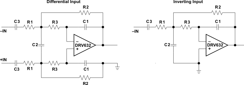
Several audio DACs used today require an external low-pass filter to remove out-of-band noise. This is possible with the DRV632, as it can be used like a standard operational amplifier. Several filter topologies can be implemented, both single-ended and differential. In Figure 8, multi-feedback (MFB) with differential input and single-ended input are shown.
An ac-coupling capacitor to remove dc content from the source is shown; it serves to block any dc content from the source and lowers the dc gain to 1, helping to reduce the output dc offset to a minimum.
To calculate the component values, use the TI WEBENCH® Filter Designer (www.ti.com/filterdesigner).
 Figure 8. Second-Order Active Low-Pass Filter
 The resistor values should have a low value for obtaining low noise, but should also have a high enough value to get a small-size ac-coupling capacitor. With the proposed values of R1 = 15 kΩ, R2 = 30 kΩ, and R3 = 43 kΩ, a dynamic range (DYR) of 106 dB can be achieved with a 1-μF input ac-coupling capacitor.