ZHCSJ02A november 2018 – august 2020 DRV5057
PRODUCTION DATA
- 1
- 1 特性
- 2 应用
- 3 说明
- 4 Revision History
- 5 Pin Configuration and Functions
- 6 Specifications
- 7 Detailed Description
- 8 Application and Implementation
- 9 Power Supply Recommendations
- 10Layout
- 11Device and Documentation Support
- 12Mechanical, Packaging, and Orderable Information
8.2.1.2 Detailed Design Procedure
Linear Hall effect sensors provide flexibility in mechanical design because many possible magnet orientations and movements produce a usable response from the sensor. Figure 8-2 illustrates one of the most common orientations that uses the full north to south range of the sensor and causes a close-to-linear change in magnetic flux density as the magnet moves across the sensor. Figure 8-3 illustrates the close-to-linear change in magnetic field present at the sensor as the magnet moves a given distance across the sensor. The usable linear region is close to but less than the length (thickness) of the magnet.
When designing a linear magnetic sensing system, always consider these three variables: the magnet, sensing distance, and the range of the sensor. Select the DRV5057 with the highest sensitivity possible based on the system distance requirements without railing the sensor PWM output. To determine the magnetic flux density the sensor receives at the various positions of the magnet, use a magnetic field calculator or simulation software, referring to magnet specifications, and testing.
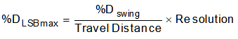
Determine if the desired accuracy is met by comparing the maximum allowed duty cycle least significant bit (%DLSBmax) with the noise level (PWM jitter) of the device. Equation 3 calculates the %DLSBmax by taking into account the used length of the linear region (travel distance), the desired resolution, and the output PWM swing (within the linear duty cycle range).
Thus, with this example (and a linear duty cycle range of 8%D to 92%D), using Equation 3 gives (92 – 8) / (10) × 0.1 = 0.84%DLSBmax. This value is larger than the 0.1%D jitter, and therefore the desired accuracy can be achieved by using Equation 2 to select a %DLSB that is equal to or less than 0.84. Then, simply calibrate the magnet position to align the sensor output along the movement path.