ZHCSDW9B May 2015 – March 2016 DRV421
PRODUCTION DATA.
- 1 特性
- 2 应用
- 3 说明
- 4 修订历史记录
- 5 Pin Configuration and Functions
- 6 Specifications
-
7 Detailed Description
- 7.1 Overview
- 7.2 Functional Block Diagram
- 7.3
Feature Description
- 7.3.1 Fluxgate Sensor
- 7.3.2 Integrator-Filter Function and Compensation Loop Stability
- 7.3.3 H-Bridge Driver for Compensation Coil
- 7.3.4 Shunt Sense Amplifier
- 7.3.5 Overrange Comparator
- 7.3.6 Voltage Reference
- 7.3.7 Overload Detection and Control
- 7.3.8 Magnetic Core Demagnetization
- 7.3.9 Search Function
- 7.3.10 Error Flag
- 7.4 Device Functional Modes
- 8 Application and Implementation
- 9 Power-Supply Recommendations
- 10Layout
- 11器件和文档支持
- 12机械、封装和可订购信息
7 Detailed Description
7.1 Overview
The DRV421 is a fully-integrated, magnetic fluxgate sensor, with the necessary sensor conditioning and compensation circuitry for closed-loop current sensors. The device is inserted into an air gap of an external ferromagnetic toroid core to sense the magnetic field. A compensation coil wrapped around the magnetic core generates a magnetic field opposite to the one generated by the current flow to be measured.
At dc and low-frequencies, the magnetic field induced by the current in the primary conductor generates a flux in the magnetic core. The fluxgate sensor detects the flux in the DRV421. The device filters the sensor output to provide loop stability. The filter output connects to the built-in H-bridge driver that drives an opposing current through the external compensation coil. The compensation coil generates an opposite magnetic field that brings the original magnetic flux in the core back to zero.
At higher frequencies, the inductive coupling between the primary conductor and compensation coil directly drives a current through the compensation coil.
The compensation current is proportional to the primary current (IPRIMARY), with a value that is calculated using Equation 1:
where
- NWINDING = the number of windings of the compensation coil
This compensation current generates a voltage drop across a small external shunt resistor, RSHUNT. An integrated difference amplifier with a fixed gain of 4 V/V measures this voltage and generates an output voltage that is referenced to REFIN and proportional to the primary current. The Functional Block Diagram section shows the DRV421 used as a closed-loop current sensor, for both single-ended and differential primary currents.
7.2 Functional Block Diagram
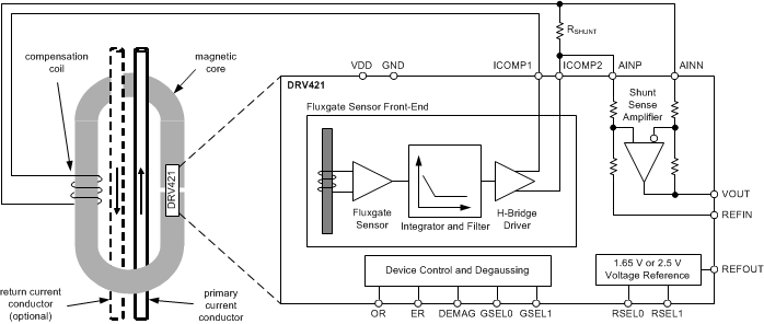
7.3 Feature Description
7.3.1 Fluxgate Sensor
The fluxgate sensor of the DRV421 is uniquely suited for closed-loop current sensors because of its high sensitivity, low noise, and low offset. The fluxgate principle relies on repeatedly driving the sensor in and out of saturation; therefore, the sensor is free of any significant magnetic hysteresis. The feedback loop accurately drives the magnetic flux inside the core to zero.
The DRV421 package is free of any ferromagnetic materials in order to prevent magnetization by external fields and to obtain accurate and hysteresis-free operation. Select nonmagnetizable materials for the printed circuit board (PCB) and passive components in the direct vicinity of the DRV421; see the Layout Guidelines section for more details.
Figure 52 shows the orientation of the fluxgate sensor and the direction of magnetic sensitivity inside of the package. This orientation is marked by a straight line on top of the package.
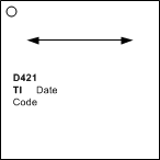 Figure 52. Orientation and Magnetic Sensitivity Direction of the Integrated Fluxgate Sensor
7.3.2 Integrator-Filter Function and Compensation Loop Stability
The DRV421 and the magnetic core are components of the system feedback loop that compensates the magnetic flux generated by the primary current. Therefore, the loop properties and stability depend on both components. Four key parameters determine the stability and effective loop gain at high frequencies:
-
GSEL[1:0] Filter gain setting pins of the DRV421
-
GCORE Open-loop, current-to-field transfer of the magnetic core
Amount of magnetic field generated by 1 A of uncompensated primary current (unit is T/A).
-
NWINDING Number of compensation coil windings
-
L Compensation coil inductance
A minimum inductance of 100 mH is required for stability. Higher inductance improves overload current robustness (see the Overload Detection and Control section).
To properly select the filter gain of the DRV421, combine these three parameters into a modified gain factor (GMOD) using Equation 2:

The effective loop gain is proportional to the current-to-field transfer of the magnetic core (larger field means larger gain) and number of compensation coil windings (larger number of windings means larger compensation field for a given input current). The compensation coil inductance adds a low-frequency pole to the system, thus a larger inductance reduces the effective loop gain at higher frequencies. A more detailed review of system loop stability is provided in application report SLOA224, Designing with the DRV421: Control Loop Stability.
For stable operation with a wide range of magnetic cores, the DRV421 features an adjustable loop filter controlled with pins GSEL1 and GSEL0. Table 1 lists the different filter settings and the related core properties. For standard closed-loop current transducer modules with medium inductance and small shunt resistor value, use gain setting 10. Gain setting 01 features a higher integrator-filter crossover frequency of 3.8 kHz, and is recommended for fault-current sensors with a large shunt resistor and medium inductance.
Table 1. DRV421 Loop Gain Filter Settings and Relation to Magnetic Core Parameters
| GSEL1 | GSEL0 | COMPENSATION LOOP PROPERTIES | RANGE OF MODIFIED GAIN FACTOR GMOD | RANGE OF COMPENSATION COIL INDUCTANCE L (NWINDING = 1000 and GCORE = 0.6 mT/A) |
|
|---|---|---|---|---|---|
| INTEGRATOR CORNER FREQUENCY | AC OPEN-LOOP GAIN | ||||
| 0 | 0 | 3.8 kHz | 8.5 | 3 < GMOD < 12 | 100 mH < L < 200 mH |
| 0 | 1 | 3.8 kHz | 38 | 1 < GMOD < 3 | 200 mH < L < 600 mH |
| 1 | 0 | 1.9 kHz | 25 | 1 < GMOD <3 | 200 mH < L < 600 mH |
| 1 | 1 | 1.9 kHz | 70 | 0.3 < GMOD < 1 | 600 mH < L < 2 H |
Table 1 gives an initial gain-setting recommendation based on a simulation model of a generic magnetic core. Secondary magnetic effects, such as eddy current losses and core hysteresis, can lead to different optimal settings. Therefore, make sure to verify the correct gain setting by measuring the response of the current sensor to an input current step at compensation driver output pins ICOMP1 and ICOMP2. Examples of measurement results with a magnetic core of 300 mH, 1000 compensation coil windings, and different DRV421 gain settings are shown in Figure 53 to Figure 56.
![DRV421 Settling of ICOMP1 and ICOMP2
with GSEL[1:0] = 00 DRV421 ai_gain00_bos704.gif](/ods/images/ZHCSDW9B/ai_gain00_bos704.gif)
with GSEL[1:0] = 00
![DRV421 Settling of ICOMP1 and ICOMP2
with GSEL[1:0] = 10 DRV421 ai_gain10_bos704.gif](/ods/images/ZHCSDW9B/ai_gain10_bos704.gif)
with GSEL[1:0] = 10
![DRV421 Settling of ICOMP1 and ICOMP2
with GSEL[1:0] = 01 DRV421 ai_gain01_bos704.gif](/ods/images/ZHCSDW9B/ai_gain01_bos704.gif)
with GSEL[1:0] = 01
![DRV421 Settling of ICOMP1 and ICOMP2
with GSEL[1:0] = 11 DRV421 ai_gain11_bos704.gif](/ods/images/ZHCSDW9B/ai_gain11_bos704.gif)
with GSEL[1:0] = 11
These measurement examples show a stable response for both GSEL[1:0] = 10 and 11 settings. However, inductive coupling between the primary current and compensation coil makes it difficult to measure high-frequency instability. Therefore, use the lowest gain setting that yields a stable response; in this case, use gain setting 10.
7.3.3 H-Bridge Driver for Compensation Coil
The H-bridge compensation coil driver provides the current for the compensation coil at pins ICOMP1 and ICOMP2. A fully-differential driver stage maximizes the driving voltage that is needed to overcome the wire resistance and inductance of the coil with a single 3.3-V or 5-V supply. The low impedance of the H-bridge driver outputs over a wide frequency range provides a smooth transition between the compensation frequency range of the integrator-filter stage and the high-frequency range of the primary current that directly couples into the compensation coil according to the winding ratio (transformer effect).
The common-mode voltage of the H-bridge driver outputs is set by the RSEL pins (see the Voltage Reference section). Thus, the common-mode voltage of the shunt sense amplifier is matched if the internal reference is used.
The two compensation driver outputs are protected and accept inductive energy. However, for high-current sensors, add external protection diodes (see the Protection Recommendations section).
Consider the polarity of the compensation coil connection to the output of the H-bridge driver. If the polarity is incorrect, the H-bridge output drives to the power supply rails, even at low primary-current levels. In this case, interchange the connection of pins ICOMP1 and ICOMP2 to the compensation coil.
7.3.4 Shunt Sense Amplifier
The compensation coil current creates a voltage drop across the external shunt resistor, RSHUNT. The internal differential amplifier senses this voltage drop. This differential amplifier offers wide bandwidth and a high slew rate for fast current sensors. Excellent dc stability and accuracy result from an autozero technique. The voltage gain is 4 V/V, set by precisely-matched and thermally-stable internal resistors.
Both AINN and AINP differential amplifier inputs are connected to the shunt resistor. This resistor, in series with the internal 10-kΩ resistor, affects the overall gain and causes an additional gain error; this gain error is often negligible. However, if a common-mode rejection of 70 dB is desired, the match of both divider ratios must be higher than 1/3000. Therefore, for best common-mode rejection performance, place a dummy shunt resistor (R5) with a value higher than the shunt resistor in series with the REFIN pin to restore matching of both resistor dividers, as shown in Figure 57.
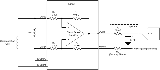 Figure 57. Internal Difference Amplifier with Example of a Decoupling Filter
For an overall gain of 4 V/V, calculate the value of R5 using Equation 3:

where
- R2 / R1 = R4 / R3 = 4
- R5 = RSHUNT × 4
If the input signal is large, the amplifier output drives close to the supply rails. The amplifier output is able to drive the input of a successive approximation register (SAR) analog-to-digital converter (ADC). For best performance, add an RC low-pass filter stage between the shunt sense amplifier output and the ADC input. This filter limits the noise bandwidth and decouples the high-frequency sampling noise of the ADC input from the amplifier output. For filter resistor RF and filter capacitor CF values, refer to the specific converter recommendations in the respective product data sheet.
The shunt sense amplifier output drives 100 pF directly and shows 50% overshoot with a 1-nF capacitance. Filter resistor RF extends the capacitive load range. Note that with an RF of only 20 Ω, the load capacitor must be either less than 1 nF or more than 33 nF to avoid overshoot; with an RF of 50 Ω, this transient area is avoided.
Reference input REFIN is the common-mode voltage node for output signal VOUT. Use the internal voltage reference of the DRV421 by connecting the REFIN pin to reference output REFOUT. To avoid mismatch errors, use the same reference voltage for REFIN and the ADC. Alternatively, use an ADC with a pseudodifferential input, with the positive input of the ADC connected to the VOUT and the negative input connected to REFIN of the DRV421.
7.3.5 Overrange Comparator
High peak current across the shunt resistor can generate a voltage drop that overloads the shunt sense amplifier input. The open-drain, active-low output overrange pin (OR) indicates an overvoltage condition of the amplifier. The output of this flag is suppressed for 3 μs, preventing unwanted triggering from transients and noise. This pin returns to high as soon as the overload condition is removed; an external pull-up resistor is required to return the OR pin to high.
This OR output can be used as a window comparator to actively shut off circuits in the system. The value of the shunt resistor defines the operating window for the current, and sets the ratio between the nominal signal and the trip level of the overrange comparator. The trip level (IMAX) of this window comparator is calculated using Equation 4:
where
- Input Voltage Swing = Output Voltage Swing / Gain
For example, with a 5-V supply, the output voltage swing is approximately ±2.45 V (load and supply voltage-dependent).
The gain of 4 V/V enables an input voltage swing of ±0.6125 V.
The resulting trip level is IMAX = 0.6125 V / RSHUNT.
See Figure 32 and Figure 33 in the Typical Characteristics section for details.
Common window comparators use a preset level to detect an overrange condition. The DRV421 internally detects an overrange condition as soon as the amplifier exceeds the linear operating range, not just at a preset voltage level. Therefore, the error is reliably indicated in faults such as output-short, low-load, or low-supply conditions. This configuration is a safety improvement if compared to a standard voltage-level comparator.
The internal resistance of the compensation coil may prevent high compensation current flow because of H-bridge driver overload; therefore, the shunt sense amplifier might not overload. However, a fast rate of change of the primary current transmitted through transformer effect safely triggers the overload flag.
7.3.6 Voltage Reference
The internal precision voltage reference circuit offers low drift performance at the REFOUT output pin and is used for internal biasing. The reference output is intended to be the common-mode voltage of the output (VOUT pin) to provide a bipolar signal swing. This low-impedance output tolerates sink and source currents of ±5 mA. However, fast load transients can generate ringing on this line. A small series resistor of a few ohms improves the response, particularly for capacitive loads equal to or greater than 1 μF.
Adjust the value of the voltage reference output to the power supply of the DRV421 using mode selection pins RSEL0 and RSEL1, as shown in Table 2.
Table 2. Reference Output Voltage Selection
| MODE | RSEL1 | RSEL0 | DESCRIPTION |
|---|---|---|---|
| VREFOUT = 2.5 V | 0 | 0 | Use with sensor module supply of 5 V |
| VREFOUT = 1.65 V | 0 | 1 | Use with sensor module supply of 3.3 V |
| Ratiometric output | 1 | x | Provides output centered on VDD / 2 |
In ratiometric output mode, an internal resistor divider divides the power supply voltage by a factor of two.
For current sensor modules with a reference input pin, the DRV421 also allows overwriting the internal reference with an external reference voltage, VEXT, as shown in Figure 58. If there is a significant difference between the external and the internal voltage, resistor R5 limits the current flow from the internal reference. In this case, the internal reference sources current IREFOUT shown in Equation 5:

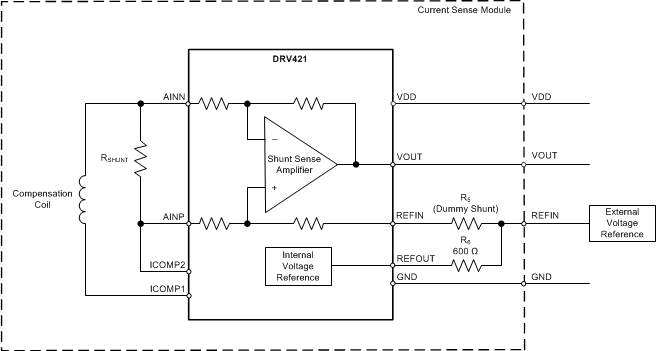 Figure 58. DRV421 with External Reference
The example of 600 Ω for R6 was chosen for illustration purposes; different values are possible. If no external reference is connected, R6 has little impact on the common-mode rejection of the shunt sense amplifier; therefore, use a resistor value that is as small as possible.
7.3.7 Overload Detection and Control
Magnetic fluxgate sensors have a very high sensitivity and allow detection of small magnetic fields. These sensors are ideally suited for use in closed-loop current modules appllications because the high sensitivity makes sure that the field inside the core gap is accurately driven to zero. However, for large fields, the fluxgate saturates and causes the output to return to zero, as shown in Figure 59.
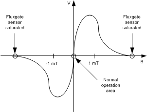 Figure 59. Typical Fluxgate Sensor Response to Magnetic Fields
In normal operation, the feedback loop keeps the magnetic field close to zero. However, large overload currents that exceed the measurement range (for example, short-circuit currents) saturates the fluxgate. The behavior is shown in Figure 60, where the compensation current, magnetic field in the core, and fluxgate output are shown for the case of a 1000-A primary current step.
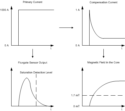 Figure 60. Closed-Loop Current Sensor Response to an Overloaded Step Current
Use the inverse of Equation 1 to calculate the current measurement range. For example, if the compensation coil has 1000 windings, the maximum measurement range is 210 A at a 5-V supply (210-mA minimum compensation driver capability × 1000 windings). The inductive coupling between primary current and compensation coil initially provides a correct compensation current. However, over time, the compensation current drops to 210 mA and the field inside the core increases beyond the measurement range of the fluxgate. Thus, the sensor output returns to zero because of saturation.
This zero output causes unpredictable behavior in the analog control loop. For example, as a result of an invalid fluxgate output, the H-bridge drives the wrong compensation current and generates a large magnetic field through the compensation coil. This magnetic field keeps the fluxgate in saturation and leads to system lockup. This unpredicatable behavior exists for any fluxgate-based current sensor.
For proper handling of overload currents, the DRV421 features a two-step overload detection and control function. Firstly, the polarity of the last four fluxgate sensor outputs exceeding a threshold value of approximately 13 µT are internally stored. Secondly, the DRV421 features an additional circuitry that verifies every 4 µs whether the fluxgate is saturated. If saturation is detected, digital circuitry overrides the fluxgate output and provides a high output according to the polarity detected during the last valid sensor output. As a result, the H-brigde drives the outputs to the supply rails, making sure that the magnetic field returns to within the fluxgate range as soon as the current returns to within the measurement range. After this happens, the fluxgate is no longer saturated, and normal analog feedback loop operation resumes. During fluxgate saturation, the error pin is pulled low to signal that the current exceeds the measurement range (see the Error Flag section).
For correct operation of this overload control feature, at least 10 µs are required between the time the field exceeds the polarity detection threshold (13 µT) and the saturation trip level (1.7 mT). Initially, fast primary current steps are inductively coupled to the compensation coil (transformer effect); therefore, the primary current rise time is not limited. Instead, the rise time is determined by the compensation coil inductance; a larger inductance leads to a slower compensation current decrease. The minimum required inductance is 100 mH; for optimal robustness, use 300 mH (see the Magnetic Core Design section for detailed requirements).
7.3.8 Magnetic Core Demagnetization
Ferromagnetic cores can have a significant remanence (residual magnetism in the absence of any currents). This core magnetization is caused by strong external magnetic fields, overcurrent conditions in the system, or if a significant primary current flows when the sensor is not powered. This remaining magnetic field is indistinguishable from an actual primary current, and creates a magnetic offset error. This magnetic offset error limits the precision and the dynamic range of the current sensor, and is independent of the fluxgate sensor front-end offset specified in this data sheet.
To reduce errors caused by core magnetization, the DRV421 features a unique closed-loop demagnetization feature. Conventional open-loop demagnetization techniques rely on driving a fixed ac waveform through the compensation coil. Instead, the DRV421 demagnetization feature first measures the magnetic offset using its integrated fluxgate sensor, and then drives a controlled ac waveform to reduce the measured magnetization. This method results in significantly better results. Moreover, any fluxgate offset is part of the closed-loop demagnetization measurement, and therefore removed along with core magnetization, leaving only fluxgate offset drift over temperature as an error source.
Start the demagnetization feature on demand by pulling the DEMAG pin high for at least 25 µs. This process starts a 500-ms demagnetization cycle. During this time, the error pin (ER) is pulled low to indicate that the output is not valid. When DEMAG is high during power up, the demagnetization cycle initiates immediately after the supply voltage crosses the power-up threshold. Hold DEMAG low to avoid this cycle during start up. To abort the demagnetization cycle, pull DEMAG low for longer than 25 µs. Figure 61 shows the ICOMPx output behavior during a demagnetization sequence. Figure 62 shows the reduced error resulting from core demagnetization.
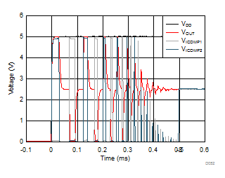 Figure 61. Demagnetization Sequence
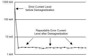
During a demagnetization cycle, the primary current must be zero because the resulting magnetic field cannot be distinguished from the remanence of the core. A demagnetization cycle in the presence of primary current (or any other sources of magnetic field) leads to residual errors because the demagnetization feature attempts to reduce the primary-generated field to zero, but significantly magnetizes the core instead of demagnetizing the core. If a primary current is present that is large enough to saturate the fluxgate sensor during start up, the DRV421 skips demagnetization (regardless of the level on the DEMAG pin), and the search function starts instead (see the Search Function section for more details).
To reduce effects from the earth's magnetic field, degauss in the same orientation as nominal operation of the system.
7.3.9 Search Function
Closed-loop current sensors usually require primary current to be applied only after the sensor is powered up. This requirement allows the feedback loop to start from zero current operation; the magnetic core is maintained at zero flux at all times, thus preventing magnetization. Moreover, the DRV421 integrated fluxgate has a limited measurement range of 1.7 mT. As a result, the presence of a significant primary current at power up saturates the fluxgate, and the system feedback loop does not work; similar to the presence of an overload current (see the Overload Detection and Control section).
The DRV421 search function allows for a power up in presence of primary dc current. If the fluxgate is saturated at power up, the digital logic of the DRV421 connects ICOMP1 to VDD and COMP2 to GND for 30 ms. Because of the compensation coil inductance, the compensation current slowly increases during this time, and depending on the primary current polarity, may at some point compensate the primary current. In this case, the fluxgate sensor desaturates and normal operation initiates. If the fluxgate sensor is still saturated after 30 ms, the voltage polarity on ICOMPx pins is inverted (ICOMP1 = GND, ICOMP2 = VDD) and the process repeats for opposite primary current polarity. If the fluxgate remains saturated after 60 ms, the error state persists and the error pin ER remains active low. Figure 63 shows a search sequence starting with the wrong polarity.
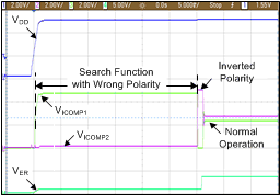 Figure 63. Search Sequence Starting with Wrong Polarity
The search funciton cannot be used for primary ac currents. Moreover, the presence of primary current before the sensor is powered up may lead to core magnetization, and thus offset shift. Therefore, for robust operation, do not power up in the presence of primary currents.
7.3.10 Error Flag
The DRV421 features an error output (ER pin) that is activated under multiple conditions. The error flag is active when the output voltage is not proportional to the primary current; during a power fail or brownout; during a demagnetization cycle; or when the magnetic field on the fluxgate is greater than 1.7 mT (saturation of the fluxgate). Saturation is usually caused by either the consequence of an overload current (see the Overload Detection and Control section) or results from a power-up in the presence of a primary current (see the Search Function section).
The error flag resets as soon as the error condition is no longer present and the circuit has returned to normal operation. The error flag is an open-drain logic output. Connect the error flag to the overrange flag for a wired-OR; for proper operation, use an external pull-up resistor. The following conditions result in error flag activation (ER asserts low):
- For 80 µs after power-up
- If a supply-voltage brownout condition (VDD < 2.4 V) lasts for more than 20 µs
- If the sensed magnetic field is > 1.7 mT because:
- Overload control is active
- Search function is active
- Demagnetization cycle is active (see the Magnetic Core Demagnetization section)
7.4 Device Functional Modes
The DRV421 has a single functional mode and is operational when the power-supply voltage is greater than 3 V. The maximum power supply voltage for the DRV421 is 5.5 V.