ZHCSIF8H December 2015 – March 2024 DLPC230-Q1 , DLPC231-Q1
PRODUCTION DATA
- 1
- 1 特性
- 2 应用
- 3 说明
- 4 Pin Configuration and Functions
-
5 Specifications
- 5.1 Absolute Maximum Ratings
- 5.2 ESD Ratings
- 5.3 Recommended Operating Conditions
- 5.4 Thermal Information
- 5.5 Electrical Characteristics
- 5.6 Electrical Characteristics for Fixed Voltage I/O
- 5.7 DMD High-Speed SubLVDS Electrical Characteristics
- 5.8 DMD Low-Speed SubLVDS Electrical Characteristics
- 5.9 OpenLDI LVDS Electrical Characteristics
- 5.10 Power Dissipation Characterisics
- 5.11 System Oscillators Timing Requirements
- 5.12 Power Supply and Reset Timing Requirements
- 5.13 Parallel Interface General Timing Requirements
- 5.14 OpenLDI Interface General Timing Requirements
- 5.15 Parallel/OpenLDI Interface Frame Timing Requirements
- 5.16 Host/Diagnostic Port SPI Interface Timing Requirements
- 5.17 Host/Diagnostic Port I2C Interface Timing Requirements
- 5.18 Flash Interface Timing Requirements
- 5.19 TPS99000-Q1 SPI Interface Timing Requirements
- 5.20 TPS99000-Q1 AD3 Interface Timing Requirements
- 5.21 DLPC23x-Q1 I2C Port Interface Timing Requirements
- 5.22 Chipset Component Usage Specification
- 6 Parameter Measurement Information
-
7 Detailed Description
- 7.1 Overview
- 7.2 Functional Block Diagram
- 7.3
Feature Description
- 7.3.1 Parallel Interface
- 7.3.2 OpenLDI Interface
- 7.3.3 DMD (SubLVDS) Interface
- 7.3.4 Serial Flash Interface
- 7.3.5 Serial Flash Programming
- 7.3.6 Host Command and Diagnostic Processor Interfaces
- 7.3.7 GPIO Supported Functionality
- 7.3.8 Built-In Self Test (BIST)
- 7.3.9 EEPROMs
- 7.3.10 Temperature Sensor
- 7.3.11 Debug Support
- 7.4 Device Functional Modes
-
8 Application and Implementation
- 8.1 Application Information
- 8.2 Typical Application
- 8.3 Power Supply Recommendations
- 8.4
Layout
- 8.4.1
Layout Guidelines
- 8.4.1.1 PCB Layout Guidelines for Internal ASIC PLL Power
- 8.4.1.2 DLPC23x-Q1 Reference Clock
- 8.4.1.3 DMD Interface Layout Considerations
- 8.4.1.4 General PCB Recommendations
- 8.4.1.5 General Handling Guidelines for Unused CMOS-Type Pins
- 8.4.1.6 Maximum Pin-to-Pin, PCB Interconnects Etch Lengths
- 8.4.1.7 Number of Layer Changes
- 8.4.1.8 Stubs
- 8.4.1.9 Terminations
- 8.4.1.10 Routing Vias
- 8.4.1.11 Layout Examples
- 8.4.2 Thermal Considerations
- 8.4.1
Layout Guidelines
- 9 Device and Documentation Support
- 10Revision History
- 11Mechanical, Packaging, and Orderable Information
5.8 DMD Low-Speed SubLVDS Electrical Characteristics
over operating free-air temperature range (unless otherwise noted)
| PARAMETER | MIN | NOM | MAX | UNIT | ||
|---|---|---|---|---|---|---|
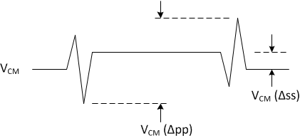
| VCM | Steady-state common mode voltage | 1.8V SubLVDS (I/O type 4,5) | 0.8 | 0.9 | 1.0 | V |
| VCM (Δpp)(1) | VCM change peak-to-peak (during switching) | 1.8V SubLVDS (I/O type 4,5) | 75 | mV | ||
| VCM (Δss)(1) | VCM change steady state | 1.8V SubLVDS (I/O type 4,5) | –10 | 10 | mV | |
| |VOD|(2) | Differential output voltage magnitude. RBGR = 75kΩ. | 1.8V SubLVDS (I/O type 4,5) | 155 | 200 | 250 | mV |
| VOD (Δ)(3) | VOD change (between logic states) | 1.8V SubLVDS (I/O type 4,5) | –10 | 10 | mV | |
| VOH | Single-ended output voltage high | 1.8V SubLVDS (I/O type 4,5) | 0.88 | 1.00 | 1.125 | V |
| VOL | Single-ended output voltage low | 1.8V SubLVDS (I/O type 4,5) | 0.675 | 0.80 | 0.925 | V |
| tR(2) | Differential output rise time | 1.8V SubLVDS (I/O type 4,5) | 250 | ps | ||
| tF(2) | Differential output fall time | 1.8V SubLVDS (I/O type 4,5) | 250 | ps | ||
| tMAX | Max switching rate | 1.8V SubLVDS (I/O type 4,5) | 240 | Mbps | ||
| DCout | Output duty cycle | 1.8V SubLVDS (I/O type 4,5) | 45% | 50% | 55% | |
| Txterm | Internal differential termination | 1.8V SubLVDS (I/O type 4,5) | 80 | 100 | 120 | Ω |
(1) Definition of VCM changes:
(2) Note that VOD is the differential voltage swing
measured across a
100Ω
termination resistance connected directly between the transmitter differential
pins. |VOD| is the magnitude of the peak to peak voltage swing across
the P and N output pins. Because VCM cancels out when measured
differentially, VOD voltage swings relative to 0. Rise and fall times
are defined for the differential VOD signal as follows:
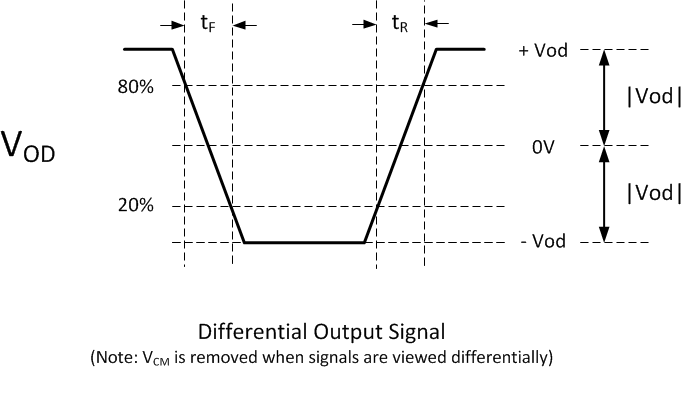
(3) When TX data input = '1', differential output voltage
VOD1 is defined. When TX data input = '0', differential output
voltage VOD0 is defined. As such, the steady state magnitude of the
difference is: |VOD| (Δ) = ||VOD1|
–
|VOD0||.