ZHCSN33B November 2017 – February 2023 DLP550JE
PRODUCTION DATA
- 1 特性
- 2 应用
- 3 说明
- 4 Revision History
- 5 Pin Configuration and Functions
-
6 Specifications
- 6.1 Absolute Maximum Ratings
- 6.2 Storage Conditions
- 6.3 ESD Ratings
- 6.4 Recommended Operating Conditions
- 6.5 Thermal Information
- 6.6 Electrical Characteristics
- 6.7 Timing Requirements
- 6.8 Window Characteristics
- 6.9 System Mounting Interface Loads
- 6.10 Micromirror Array Physical Characteristics
- 6.11 Micromirror Array Optical Characteristics
- 6.12 Chipset Component Usage Specification
- 7 Detailed Description
- 8 Application and Implementation
- 9 Power Supply Recommendations
- 10Device and Documentation Support
- 11Mechanical, Packaging, and Orderable Information
6.7 Timing Requirements
Over operating free-air temperature range (unless otherwise noted).
| MIN | NOM | MAX | UNIT | ||
|---|---|---|---|---|---|
| LVDS#T4989946-35 | |||||
| tc | Clock Cycle for DLCK_A | 3.03 | ns | ||
| tc | Clock Cycle for DCLKC_B | 3.03 | ns | ||
| tw | Pulse Duration DCLK_A | 1.36 | 1.52 | ns | |
| tw | Pulse Duration for DCLK_B | 1.36 | 1.52 | ns | |
| tSU | Setup Time, D_A[0:15] before DCLK_A | 0.35 | ns | ||
| tSU | Setup Time, D_B[0:15] before DCLK_B | 0.35 | ns | ||
| tSU | Setup Time, SCTRL_A before DCLK_A | 0.35 | ns | ||
| tSU | Setup Time, SCTRL_B before DCLK_B | 0.35 | ns | ||
| tH | Hold Time, D_A[0:15] after DCLK_A | 0.35 | ns | ||
| tH | Hold Time, D_B[0:15] after DCLK_B | 0.35 | ns | ||
| tH | Hold Time, SCTRL_A after DCLK_A | 0.35 | ns | ||
| tH | Hold Time, SCTRL_B after DCLK_B | 0.35 | ns | ||
| tskew | Channel B relative to Channel A#T4989946-36#T4989946-37 | –1.51 | 1.51 | ns | |
(1) See #DLPS0952F2 for timing requirements for LVDS.
(2) Channel A (Bus A) includes the following LVDS pairs: DCLK_AN and DCLK_AP, SCTRL_AN and SCTRL_AP, D_AN(15:0) and D_AP(15:0).
(3) Channel B (Bus B) includes the following LVDS pairs: DCLK_BN and DCLK_BP, SCTRL_BN and SCTRL_BP, D_BN(15:0) and D_BP(15:0).
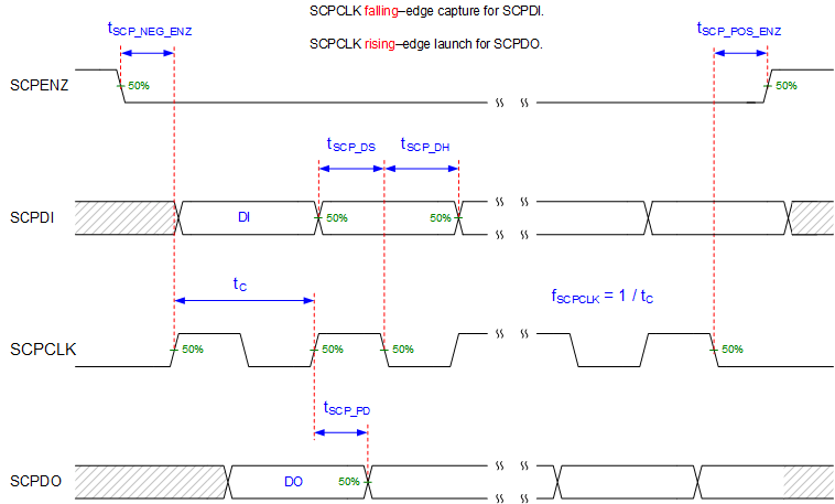 Figure 6-2 SCP Timing Parameters
Not to scale
Refer to GUID-B0CCC92B-1768-4A99-BB7C-8E88C03ABC21.html#GUID-B0CCC92B-1768-4A99-BB7C-8E88C03ABC21 for list of LVDS pins and SCP pins.
Figure 6-3 Rise Time and Fall Time Figure 6-4 Test Load Circuit for Output Propagation Measurement
For output timing analysis, the tester pin electronics and its transmission line effects must be taken into account. System design should use IBIS or other simulation tools to correlate the timing reference load to a system environment. See #T4989946-26.
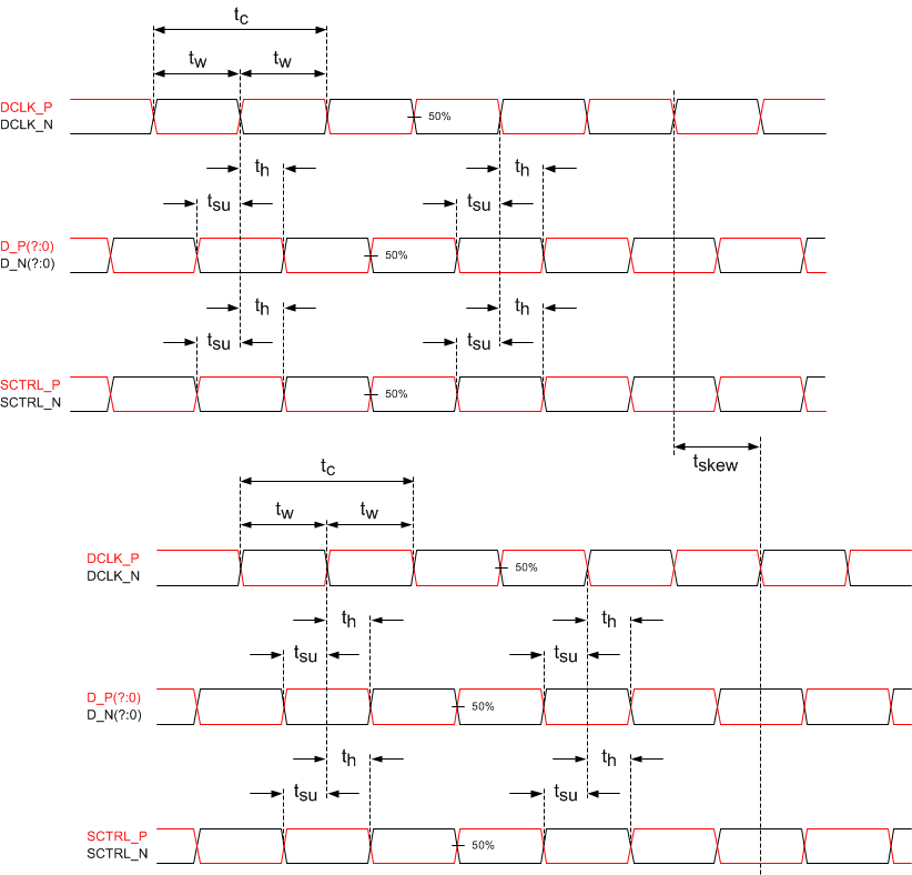 Figure 6-5 Timing Requirements
 Figure 6-6 Serial Communications Bus Waveform Requirements
Refer to LVDS Interface section
of GUID-4099E5F6-AAA6-418E-9C70-AB9F6B9ED0B7.html#GUID-4099E5F6-AAA6-418E-9C70-AB9F6B9ED0B7.
Refer to GUID-B0CCC92B-1768-4A99-BB7C-8E88C03ABC21.html#GUID-B0CCC92B-1768-4A99-BB7C-8E88C03ABC21 for list of LVDS pins.
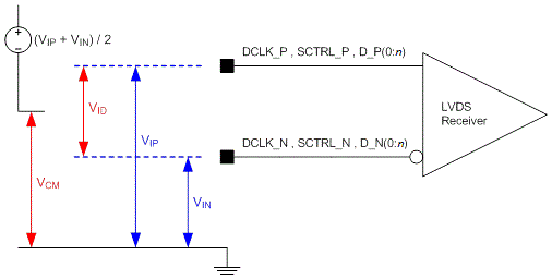
Figure 6-7 LVDS Voltage Definitions (References)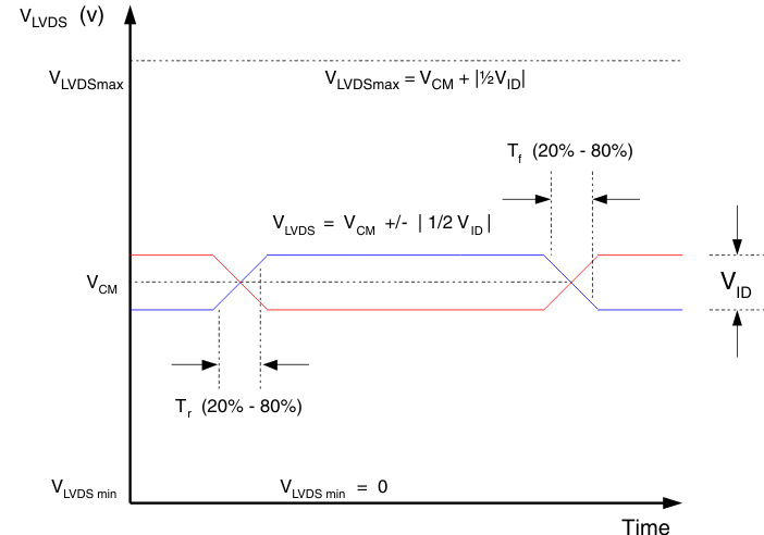
Not to scale
Refer to LVDS Interface section
of the GUID-4099E5F6-AAA6-418E-9C70-AB9F6B9ED0B7.html#GUID-4099E5F6-AAA6-418E-9C70-AB9F6B9ED0B7.
Figure 6-8 LVDS Voltage Parameter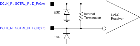
Refer to LVDS Interface section
of the GUID-4099E5F6-AAA6-418E-9C70-AB9F6B9ED0B7.html#GUID-4099E5F6-AAA6-418E-9C70-AB9F6B9ED0B7.
Refer to GUID-B0CCC92B-1768-4A99-BB7C-8E88C03ABC21.html#GUID-B0CCC92B-1768-4A99-BB7C-8E88C03ABC21 for list of LVDS pins.
Figure 6-9 LVDS Equivalent Input Circuit