ZHCSSI1D august 2008 – august 2023 DAC5311 , DAC6311 , DAC7311
PRODUCTION DATA
- 1
- 1 特性
- 2 应用
- 3 说明
- 4 Revision History
- 5 Device Comparison
- 6 Pin Configuration and Functions
-
7 Specifications
- 7.1 Absolute Maximum Ratings
- 7.2 ESD Ratings
- 7.3 Recommended Operating Conditions
- 7.4 Thermal Information
- 7.5 Electrical Characteristics
- 7.6 Timing Requirements
- 7.7 Timing Diagrams
- 7.8 Typical Characteristics: AVDD = 5 V
- 7.9 Typical Characteristics: AVDD = 3.6 V
- 7.10 Typical Characteristics: AVDD = 2.7 V
- 8 Detailed Description
- 9 Application and Implementation
- 10Device and Documentation Support
- 11Mechanical, Packaging, and Orderable Information
9.2.1.2 Detailed Design Procedure
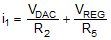
Amplifier U1 uses negative feedback to make sure that the potentials at the inverting (V–) and noninverting (V+) input terminals are equal. In this configuration, V– is directly tied to the local GND; therefore, the potential at the noninverting input terminal is driven to local ground. Thus, the voltage difference across R2 is the DAC output voltage (VOUT), and the voltage difference across R5 is the regulator voltage (VREG). These voltage differences cause currents to flow through R2 and R5, as illustrated in Figure 9-5.
 Figure 9-5 Voltage to Current Conversion
The currents from R2 and R5 sum into i1 (defined in Equation 2), and i1 flows through R3.
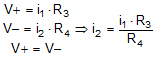
Amplifier U2 drives the base of Q1, the NPN bipolar junction transistor (BJT), to allow current to flow through R4 so that the voltage drops across R3 and R4 remain equal. This design keeps the inverting and noninverting terminals at the same potential. A small part of the current through R4 is sourced by the quiescent current of all of the components used in the transmitter design (regulator, amplifier, and DAC). The voltage drops across R3 and R4 are equal; therefore, different-sized resistors cause different current flow through each resistor. Use these different-sized resistors to apply gain to the current flow through R4 by controlling the ratio of resistor R3 to R4, as shown in Equation 3:
The current gain in the circuit helps allow a majority of the output current to come directly from the loop through Q1 instead of from the voltage-to-current converter. This current gain, in addition to the low-power components, keeps the current consumption of the voltage-to-current converter low. Currents i1 and i2 sum to form output current iout, as shown in Equation 4:

The complete transfer function, arranged as a function of input code, is shown in Equation 5. The remaining sections divide this circuit into blocks for simplified discussion.
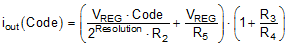
Resistor R6 is included to reduce the gain of transistor Q1, and therefore, reduce the closed-loop gain of the voltage-to-current converter for a stable design. Size resistors R2, R3, R4, and R5 based on the full-scale range of the DAC, regulator voltage, and the desired current output range of the design.