ZHCSSI1D august 2008 – august 2023 DAC5311 , DAC6311 , DAC7311
PRODUCTION DATA
- 1
- 1 特性
- 2 应用
- 3 说明
- 4 Revision History
- 5 Device Comparison
- 6 Pin Configuration and Functions
-
7 Specifications
- 7.1 Absolute Maximum Ratings
- 7.2 ESD Ratings
- 7.3 Recommended Operating Conditions
- 7.4 Thermal Information
- 7.5 Electrical Characteristics
- 7.6 Timing Requirements
- 7.7 Timing Diagrams
- 7.8 Typical Characteristics: AVDD = 5 V
- 7.9 Typical Characteristics: AVDD = 3.6 V
- 7.10 Typical Characteristics: AVDD = 2.7 V
- 8 Detailed Description
- 9 Application and Implementation
- 10Device and Documentation Support
- 11Mechanical, Packaging, and Orderable Information
9.2.3 Bipolar Operation Using the DACx311
The DACx311 has been designed for single-supply operation but a bipolar output range is also possible using the circuit in Figure 9-9. The circuit shown gives an output voltage range of ±5 V. Rail-to-rail operation at the amplifier output is achievable using an OPA211, OPA340, or OPA703 as the output amplifier. For a full list of available operational amplifiers from TI, see the TI web site at www.ti.com
The output voltage for any input code can be calculated as follows:
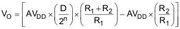
where
- n = resolution in bits; either 8 (DAC5311), 10 (DAC6311), or 12 (DAC7311).
- D = decimal equivalent of the binary code that is loaded to the DAC register. D ranges from 0 to 255 for 8-bit DAC5311, 0 to 1023 for the 10-bit DAC6311 and 0 to 4095 for the 12-bit DAC7311.
With AVDD = 5 V, R1 = R2 = 10 kΩ:

The resulting output voltage range is ±5 V. Code 000h corresponds to a –5-V output and FFFh (12-bit level) corresponding to a +5-V output.
 Figure 9-9 Bipolar Operation With the DACx311