ZHCSHA9B August 2017 – January 2018 DAC5672A
PRODUCTION DATA.
- 1 特性
- 2 应用
- 3 说明
- 4 修订历史记录
- 5 Pin Configuration and Functions
-
6 Specifications
- 6.1 Absolute Maximum Ratings
- 6.2 ESD Ratings
- 6.3 Recommended Operating Conditions
- 6.4 Thermal Information
- 6.5 Electrical Characteristics
- 6.6 Electrical Characteristics
- 6.7 Electrical Characteristics: AC Characteristics
- 6.8 Electrical Characteristics: Digital Characteristics
- 6.9 Switching Characteristics
- 6.10 Typical Characteristics
- 7 Detailed Description
- 8 Application and Implementation
- 9 Power Supply Recommendations
- 10Layout
- 11器件和文档支持
- 12机械、封装和可订购信息
7.3.3 Single-Bus Interleaved Data Interface and Timing
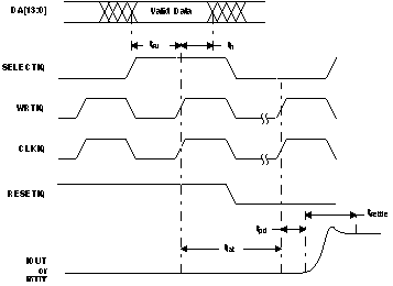
In single-bus interleaved mode, the MODE pin is connected to DGND. Figure 18 shows the timing diagram. In interleaved mode, the A- and B-channels share the write input (WRTIQ) and update clock (CLKIQ and internal CLKDACIQ). Multiplexing logic directs the input word at the A-channel input bus to either the A-channel input latch (SELECTIQ is high) or to the B-channel input latch (SELECTIQ is low). When SELECTIQ is high, the data value in the B-channel latch is retained by presenting the latch output data to its input again. When SELECTIQ is low, the data value in the A-channel latch is retained by presenting the latch output data to its input.
In interleaved mode, the A-channel input data rate is twice the update rate of the DAC core. As in dual-bus mode, it is important to maintain a correct sequence of write and clock inputs. The edge-triggered flip-flops latch the A- and B-channel input words on the rising edge of the write input (WRTIQ). This data is presented to the A- and B-DAC latches on the following falling edge of the write inputs. The DAC5672A clock input is divided by a factor of two before it is presented to the DAC latches.
Correct pairing of the A- and B-channel data is done by RESETIQ. In interleaved mode, the clock input CLKIQ is divided by two, which would translate to a non-deterministic relation between the rising edges of the CLKIQ and CLKDACIQ. RESETIQ ensures, however, that the correct position of the rising edge of CLKDACIQ with respect to the data at the input of the DAC latch is determined. CLKDACIQ is disabled (low) when RESETIQ is high.
 Figure 18. Single-Bus Interleaved Mode Operation