SGLS386F January 2009 – October 2014 DAC5670-SP
PRODUCTION DATA.
- 1 Features
- 2 Applications
- 3 Description
- 4 Revision History
- 5 Description (continued)
- 6 Pin Configuration and Functions
- 7 Specifications
- 8 Detailed Description
- 9 Application and Implementation
- 10Power Supply Recommendations
- 11Layout
- 12Device and Documentation Support
- 13Mechanical, Packaging, and Orderable Information
7 Specifications
7.1 Absolute Maximum Ratings(1)
over operating free-air temperature range (unless otherwise noted)| MIN | MAX | UNIT | ||
|---|---|---|---|---|
| Supply voltage | AVDD to GND | 5 | V | |
| DA_P[13..0], DA_N[13..0], DB_P[13..0], DB_N[13..0] | Measured with respect to GND | –0.3 | AVDD + 0.3 | V |
| NORMAL, A_ONLY, A_ONLY_INV, A_ONLY_ZS | Measured with respect to GND | –0.3 | AVDD + 0.3 | V |
| DTCLK_P, DTCLK_N, DACCLK_P, DACCLK_N | Measured with respect to GND | –0.3 | AVDD + 0.3 | V |
| LVDS_HTB, INV_CLK, RESTART | Measured with respect to GND | –0.3 | AVDD + 0.3 | V |
| IOUT_P, IOUT_N | Measured with respect to GND | AVDD – 0.5 | AVDD + 1.5 | V |
| CSCAP_IN, REFIO_IN, RBIAS_IN | Measured with respect to GND | –0.3 | AVDD + 0.3 | V |
| Peak input current (any input) | 20 | mA | ||
| Maximum junction temperature | 150 | °C | ||
| Lead temperature 1.6 mm (1/16 inch) from the case for 10 s | 260 | °C | ||
(1) Stresses above those listed under Absolute Maximum Ratings may cause permanent damage to the device. Exposure to absolute maximum conditions for extended periods may degrade device reliability. These are stress ratings only, and functional operation of the device at these or any other conditions beyond those indicated under Recommended Operating Conditions is not implied. Exposure to absolute-maximum-rated conditions for extended periods may affect device reliability.
7.2 Handling Ratings
| MIN | MAX | UNIT | |||
|---|---|---|---|---|---|
| Tstg | Storage temperature range | –65 | 150 | °C | |
| V(ESD) | Electrostatic discharge | Human body model (HBM), per ANSI/ESDA/JEDEC JS-001, all pins(1) | –250 | 250 | V |
| Charged device model (CDM), per JEDEC specification JESD22-C101, all pins(2) | –250 | 250 | |||
(1) JEDEC document JEP155 states that 500-V HBM allows safe manufacturing with a standard ESD control process.
(2) JEDEC document JEP157 states that 250-V CDM allows safe manufacturing with a standard ESD control process.
7.3 Recommended Operating Conditions
over operating free-air temperature range (unless otherwise noted)| MIN | NOM | MAX | UNIT | ||
|---|---|---|---|---|---|
| GENERAL PARAMETERS | |||||
| Full-scale output current | 30 | mA | |||
| VREFIO | Input voltage range | 1.14 | 1.2 | 1.26 | V |
| AVDD | Analog supply voltage | 3 | 3.3 | 3.6 | V |
| ƒDAC | Output update rate | 2.4 | GSPS | ||
| CMOS INTERFACE (SLEEP, RESTART, INV_CLK, NORMAL, A_ONLY, A_ONLY_INV, A_ONLY_ZS) | |||||
| VIH | High-level input voltage | 2 | 3 | V | |
| VIL | Low-level input voltage | 0 | 0 | 0.8 | V |
| DIFFERENTIAL DATA INTERFACE (DA_P[13:0], DA_N[13:0], DB_P[13:0], DB_N[13:0], DTCLK_P, DTCLK_N) | |||||
| VITH | Differential input threshold | –100 | 100 | mV | |
| VICOM | Input common mode | 0.6 | 1.4 | V | |
| CLOCK INPUTS (DACCLK_P, DACCLK_N) | |||||
| |DACCLK_P – DACCLK_N| | Clock differential input voltage | 200 | 1000 | mV | |
| Clock duty cycle | 40% | 60% | |||
| VCLKCM | Clock common mode | 1 | 1.4 | V | |
7.4 Thermal Information
| THERMAL METRIC | TEST CONDITIONS | TYP | UNIT | |||
|---|---|---|---|---|---|---|
| RθJA | Junction-to-free-air thermal resistance | Non-thermally enhanced JEDEC standard PCB, per JESD-51, 51-3 | 41.3 | °C/W | ||
| RθJC | Junction-to-case thermal resistance | MIL-STD-883 test method 1012 | 3.8 | |||
7.5 DC Electrical Characteristics
TC,MIN = –55°C to TC,MAX = 125°C, typical values at 25°C, AVDD = 3 V to 3.6 V, IoutFS = 20 mA (unless otherwise noted)| PARAMETER | TEST CONDITIONS | MIN | TYP(1) | MAX | UNIT | |
|---|---|---|---|---|---|---|
| Resolution | 14 | bits | ||||
| DC ACCURACY | ||||||
| INL | Integral nonlinearity | TC,MIN to TC,MAX , ƒDAC = 640 kHz, ƒOUT = 10 kHz | –7.5 | ±1.5 | 7.5 | LSB |
| DNL | Differential nonlinearity | –0.98 | ±0.8 | 1.75 | ||
| Monotonocity | 14 | bits | ||||
| ANALOG OUTPUT | ||||||
| Offset error | Mid-code offset | –0.45 | ±0.09 | 0.45 | %FSR | |
| Gain error | With external reference | –6.0 | ±1.6 | 6 | %FSR | |
| Gain error | With internal reference | –6.0 | ±1.6 | 6 | %FSR | |
| Output compliance range | IO(FS) = 20 mA, AVDD = 3.15 to 3.45 V | AVDD – 0.5 | AVDD + 0.5 | V | ||
| Output resistance | 300(2) | kΩ | ||||
| Output capacitance | IOUT_P and IOUT_N single ended | 13.7(2) | pF | |||
| REFERENCE OUTPUT | ||||||
| Reference voltage | 1.14 | 1.2 | 1.26 | V | ||
| Reference output current | 100 | nA | ||||
| REFERENCE INPUT | ||||||
| Input resistance | 1(2) | MΩ | ||||
| Small-signal bandwidth | 1.4 | MHz | ||||
| Input capacitance | 3.2(2) | pF | ||||
| TEMPERATURE COEFFICIENTS | ||||||
| Offset drift | 75 | ppm of FSR/°C | ||||
| Gain drift | With external reference | 75 | ppm of FSR/°C | |||
| Gain drift | With internal reference | 75 | ppm of FSR/°C | |||
| Reference voltage drift | 35 | ppm/°C | ||||
| POWER SUPPLY | ||||||
| IAVDD | Analog supply current | ƒDAC = 2.4 GHz, NORMAL input mode | 560 | 650 | mA | |
| IAVDD | Sleep mode, AVDD supply current | Sleep mode (SLEEP pin high) | 150 | 180 | mA | |
| P | Power dissipation | ƒDAC = 2.4 GHz, NORMAL input mode | 1800 | 2350 | mW | |
| PSRR | Power-supply rejection ratio | AVDD = 3.15 to 3.45 V | 0.4 | 1.3 | %FSR/V | |
(1) Typicals are characterization values at 25°C and AVDD = 3.3 V. These parameters are characterized, but not production tested.
(2) Specified by design.
7.6 AC Electrical Characteristics
TC,MIN = –55°C to TC,MAX = 125°C, typical values at 25°C, AVDD = 3 to 3.6 V, IoutFS = 20 mA (unless otherwise noted)| PARAMETER | TEST CONDITIONS | MIN | TYP(1) | MAX | UNIT | ||||
|---|---|---|---|---|---|---|---|---|---|
| ANALOG OUTPUT | |||||||||
| ts(DAC) | Output setting time to 0.1% | Mid-scale transition | 3.5 | ns | |||||
| tpd | Output propagation delay | 7 DACCLK + 1.5 ns | |||||||
| tr(IOUT) | Output rise time, 10% to 90% | 280 | ps | ||||||
| tf(IOUT) | Output fall time, 90% to 10% | 280 | ps | ||||||
| AC PERFORMANCE | |||||||||
| SFDR | Spurious-free dynamic range | ƒDAC = 2.4 GSPS, ƒOUT = 100 MHz, Dual-port mode, 0 dBFS | 46 | 55 | dBc | ||||
| ƒDAC = 2.4 GSPS, ƒOUT = 200 MHz, Dual-port mode, 0 dBFS | 51 | ||||||||
| ƒDAC = 2.4 GSPS, ƒOUT = 300 MHz, Dual-port mode, 0 dBFS | 31 | 36 | |||||||
| ƒDAC = 2.4 GSPS, ƒOUT = 500 MHz, Dual-port mode, 0 dBFS | 35 | 43 | |||||||
| ƒDAC = 2.4 GSPS, ƒOUT = 500 MHz, Dual-port mode, –6 dBFS | 47 | ||||||||
| SNR | Signal-to-noise ratio | ƒDAC = 2.4 GSPS, ƒOUT = 100 MHz, Dual-port mode, 0 dBFS | 58 | 60 | dBc | ||||
| ƒDAC = 2.4 GSPS, ƒOUT = 200 MHz, Dual-port mode, 0 dBFS | 60 | ||||||||
| ƒDAC = 2.4 GSPS, ƒOUT = 300 MHz, Dual-port mode, 0 dBFS | 56 | 62 | |||||||
| ƒDAC = 2.4 GSPS, ƒOUT = 500 MHz, Dual-port mode, 0 dBFS | 51 | 58 | |||||||
| ƒDAC = 2.4 GSPS, ƒOUT = 500 MHz, Dual-port mode, –6 dBFS | 52 | ||||||||
| THD | Total harmonic distortion | ƒDAC = 2.4 GSPS, ƒOUT = 100 MHz, Dual-port mode, 0 dBFS | 45 | 52 | dBc | ||||
| ƒDAC = 2.4 GSPS, ƒOUT = 200 MHz, Dual-port mode, 0 dBFS | 50 | ||||||||
| ƒDAC = 2.4 GSPS, ƒOUT = 300 MHz, Dual-port mode, 0 dBFS | 31 | 36 | |||||||
| ƒDAC = 2.4 GSPS, ƒOUT = 500 MHz, Dual-port mode, 0 dBFS | 35 | 46 | |||||||
| ƒDAC = 2.4 GSPS, ƒOUT = 500 MHz, Dual-port mode, –6 dBFS | 44 | ||||||||
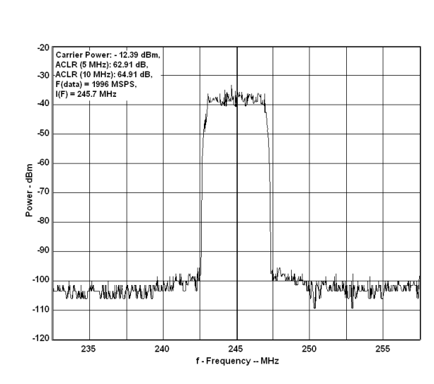
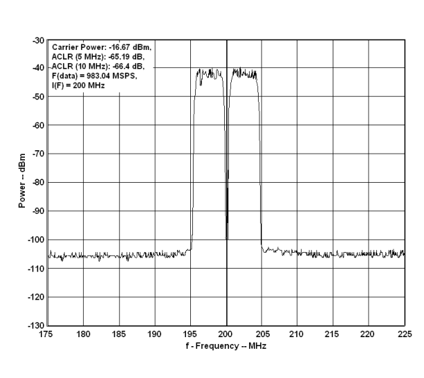
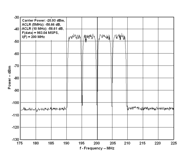
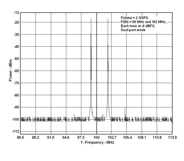
| IMD3 | Third-order two-tone intermodulation | ƒDAC = 2.4 GSPS, ƒOUT = 99 MHz and 102 MHz, Each tone at –6 dBFS, Dual-port mode. | 70 | dBc | |||||
| ƒDAC = 2.4 GSPS, ƒOUT = 200 MHz and 202 MHz, Each tone at –6 dBFS, Dual-port mode. | 68 | dBc | |||||||
| ƒDAC = 2.4 GSPS, ƒOUT = 253 MHz and 257 MHz, Each tone at –6 dBFS, Dual-port mode. | 47 | 57 | dBc | ||||||
| ƒDAC = 2.4 GSPS, ƒOUT = 299 MHz and 302 MHz, Each tone at –6 dBFS, Dual-port mode. | 35 | 55 | dBc | ||||||
| IMD | Four-tone intermodulation | ƒDAC = 2.4 GSPS, ƒOUT = 298 MHz, 299 MHz, 300 MHz, and 301 MHz, Each tone at –12 dBFS, Dual-port mode. | 47 | 62.5 | dBc | ||||
(1) Typicals are characterization values at 25°C and AVDD = 3.3 V. These parameters are characterized, but not production tested.
7.7 Digital Electrical Characteristics
TC,MIN = –55°C to TC,MAX = 125°C, typical values at 25°C, AVDD = 3 to 3.6 V, IoutFS = 20 mA (unless otherwise noted)| PARAMETER | TEST CONDITIONS | MIN | TYP(1) | MAX | UNIT | |
|---|---|---|---|---|---|---|
| CMOS INTERFACE (SLEEP, RESTART, INV_CLK, NORMAL, A_ONLY, A_ONLY_INV, A_ONLY_ZS) | ||||||
| IIH | High-level input current | 0.2 | 10 | μA | ||
| IIL | Low-level input current | –10 | –0.2 | μA | ||
| Input capacitance | 2.5(2) | pF | ||||
| DIFFERENTIAL DATA INTERFACE (DA_P[13:0], DA_N[13:0], DB_P[13:0], DB_N[13:0], DTCLK_P, DTCLK_N) | ||||||
| ZT | Internal termination impedance | 80 | 100 | 125 | Ω | |
| Ci | Input capacitance | 2.6(2) | pF | |||
(1) Typicals are characterization values at 25°C and AVDD = 3.3 V. These parameters are characterized, but not production tested.
(2) Specified by design.
(3) Tested using SNR as pass/fail criteria.
7.8 Timing Requirements
| MIN | TYP | MAX | UNIT | |||
|---|---|---|---|---|---|---|
| DIFFERENTIAL DATA INTERFACE (DA_P[13:0], DA_N[13:0], DB_P[13:0], DB_N[13:0] EXTERNAL TIMING WITH DLL IN RESTART) (See Figure 2) | ||||||
| tsetup | Data setup to DLYCLK(3) | RESTART = 1, DLYCLK 20-pF load
See Figure 2 |
4.75 | nS | ||
| thold | Data hold to DLYCLK (3) | RESTART = 1, DLYCLK 20-pF load See Figure 2 |
–3.5 | nS | ||
| DLL (See Figure 15) | ||||||
| NegD | DLL min negative delay | RESTART = 0 | 150 | ps | ||
| PosD | DLL min positive delay | RESTART = 0 | 600 | ps | ||
| tvalid | CLK/4 internal setup + hold width | 160 | ps | |||
| Fdac | RESTART = 0 | 1 | 2.4 | GHz | ||
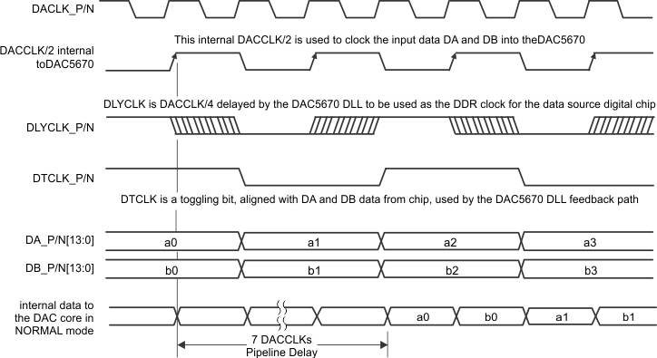 Figure 1. DLL Input Loop Functional Timing
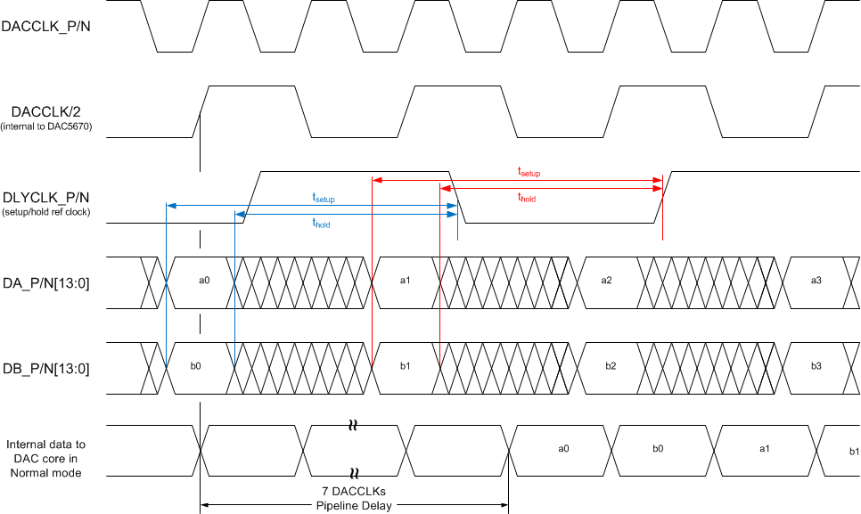 Figure 2. External Interface Timing With DLL in Restart
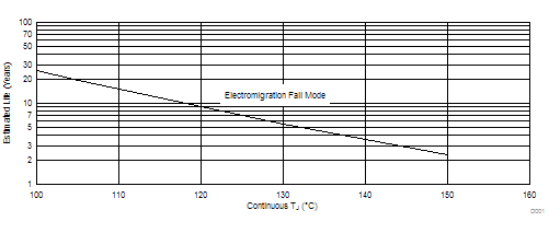
A. See data sheet for absolute maximum and minimum recommended operating conditions.
B. Silicon operating life design goal is 10 years at 105°C junction temperature (does not include package interconnect life).
Figure 3. DAC5670-SP – 192/GEM PackageOperating Life Derating Chart
7.9 Typical Characteristics