SGLS386F January 2009 – October 2014 DAC5670-SP
PRODUCTION DATA.
- 1 Features
- 2 Applications
- 3 Description
- 4 Revision History
- 5 Description (continued)
- 6 Pin Configuration and Functions
- 7 Specifications
- 8 Detailed Description
- 9 Application and Implementation
- 10Power Supply Recommendations
- 11Layout
- 12Device and Documentation Support
- 13Mechanical, Packaging, and Orderable Information
8 Detailed Description
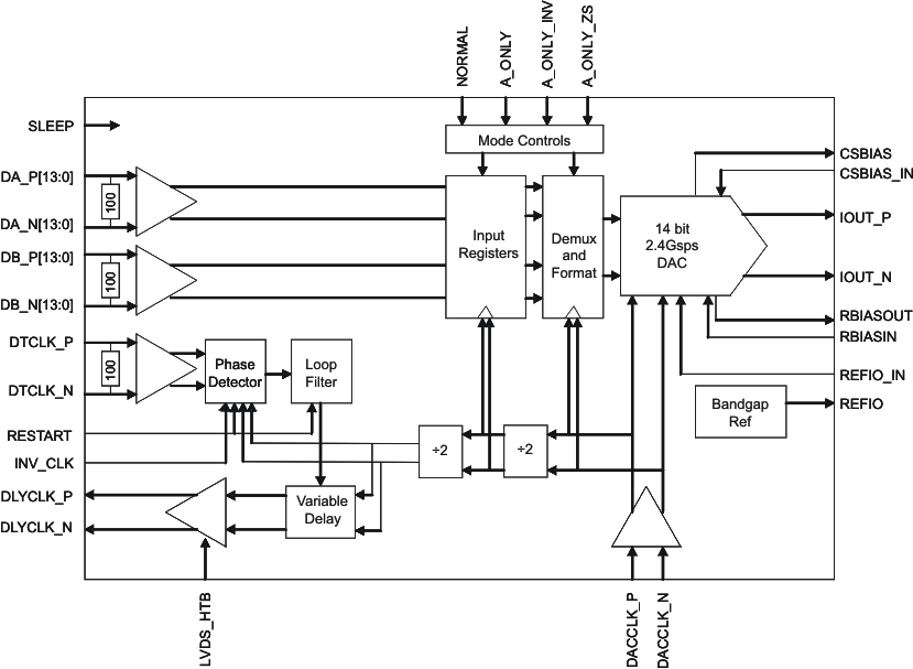
8.1 Overview
Figure 26 shows a simplified block diagram of the current steering DAC5670. The DAC5670 consists of a segmented array of NPN-transistor current sinks, capable of delivering a full-scale output current up to 30 mA. Differential current switches direct the current of each current sink to either one of the complementary output nodes IOUT_P or IOUT_N. The complementary current output enables differential operation, canceling out common-mode noise sources (digital feed-through, on-chip, and PCB noise), dc offsets, even-order distortion components, and doubling signal output power.
The full-scale output current is set using an external resistor (RBIAS) in combination with an on-chip bandgap voltage reference source (1.2 V) and control amplifier. The current (IBIAS) through resistor RBIAS is mirrored internally to provide a full-scale output current equal to 32× IBIAS. The full-scale current is adjustable from 30 mA down to 5 mA by using the appropriate bias resistor value.
8.2 Functional Block Diagram
8.3 Feature Description
8.3.1 Digital Inputs
The DAC5670 differential digital inputs are compatible with LVDS and HyperTransport voltage levels.
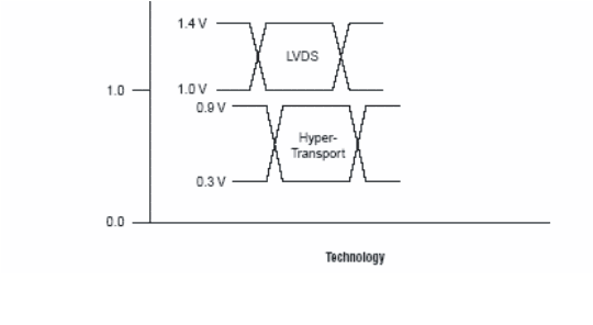 Figure 11. Digital Input Voltage Options
The DAC5670 uses low-voltage differential signaling (LVDS and HyperTransport) for the bus input interface. The LVDS and HyperTransport input modes feature a low differential voltage swing. The differential characteristic of LVDS and HyperTransport modes allow for high-speed data transmission with low electromagnetic interference (EMI) levels. Figure 12 shows the equivalent complementary digital input interface for the DAC5670, valid for pins DA_P[13:0], DA_N[13:0], DB_P[13:0], and DB_N[13:0].
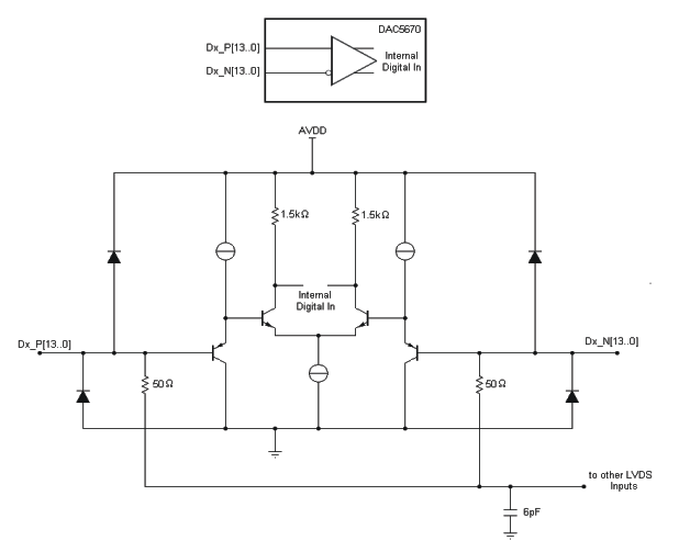 Figure 12.
Figure 13 shows a schematic of the equivalent CMOS/TTL-compatible digital inputs of the DAC5670, valid for the following pins: RESTART, LVDS_HTB, INV_CLK, SLEEP, NORMAL, A_ONLY, A_ONLY_INV, and A_ONLY_ZS.
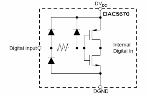 Figure 13.
8.3.2 DLL Usage
The DAC5670 is clocked at the DAC sample rate. Each input port runs at a maximum of 1.2 GSPS. The DAC5670 provides an output clock (DLYCLK) at one-half the input port data rate (DACCLK/4), and monitors an additional reference bit (DTCLK). DTCLK is used as a feedback clock to adjust interface timing. To accomplish this, the DAC5670 implements a DLL to help manage the timing interface from external data source. As with all DLLs, there are limitations on the capability of the DLL with respect to the delay chain length, implementation of the phase detector, and the bandwidth of the control loop. The DAC5670 implements a quadrature-based phase detector. This scheme allows for the DLL to provide maximum setup or hold delay margins when quadrature can be reached. Quadrature is reached when the internal CLK / 4 is 90° out of phase with DTCLK. Additionally, as the frequency of operation decreases, the delay line's fixed length limits its ability to change the delay path enough to reach quadrature (see Figure 15). Note that the delay line has asymmetric attributes. The NegD range is smaller than the PosD range. From its nominal (restart) position, it can delay more than it can subtract.
Figure 15 represents the behavior of the phase detector and the delay line with respect to initial positions of the rising edge of DTCLK. There are four distinct quadrants that define the behavior. Each quadrant represents the period of the DDR clock rate (600 MHz in the 2.4 GSPS case) divided by 4. The ideal location has the initial delays of DTCLK (and hence data bits) in quadrant 1. The stable lock point of DLL is at T / 4, between Q1 and Q2. If DTCLK's initial delay is in quadrants 3 or 4, the INV_CLK pin can be asserted to improve the ability of DLL to obtain quadrature. This assertion moves the stable quadrature point to the center of 3T / 4 vs T / 4 as shown in Figure 15. Essentially, the zones that add delay become zones that subtract delay and vice-versa. The clock phase of CLK / 4 would also invert.
In cases where it is not appropriate to use the DLL to manage the timing interface, it is possible to use fixed setup and hold values for DA and DB signals relative to the generated DLYCLK output when the DLL is held in restart. This is accomplished by asserting RESTART to logic high and using the timing input conditions for external timing interface with DLL in restart in the DLL Usage. When using external setup and hold timing, the user does not need to provide DTCLK. DTCLK should be biased to valid LVDS levels in that case (see Figure 2).
The setup/hold values are non-traditional, as they represent the setup/hold of an input to a generated clock (DLYCLK). Additionally, the setup/hold numbers represent delays that may be longer than the DACCLK or DACCLK/2 periods. To calculate the setup/hold values to the nearest adjacent DLYCLK transistion, the user must subtract multiples of DACLCK/2 periods until the setup is less than a DACCLK/2 period. The same amount can be subtracted from the hold time. These new setup/hold values will be frequency dependent.
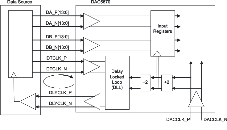 Figure 14. DLL Input Loop Simplified Block Diagram
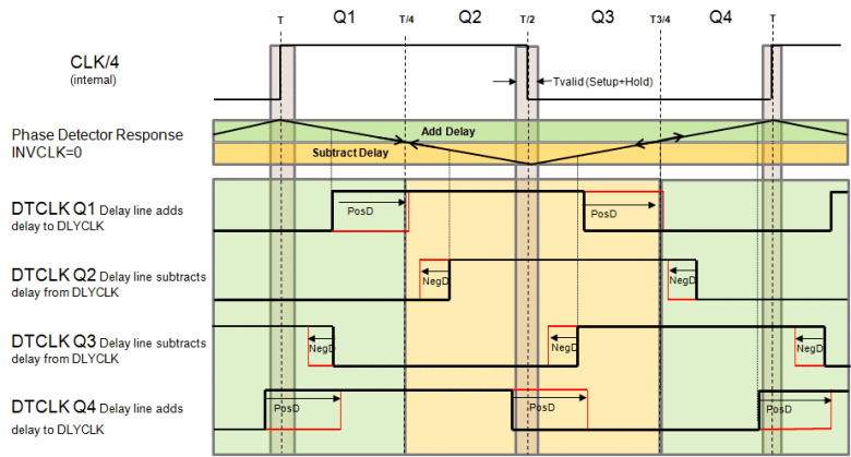 Figure 15. DLL Phase Detector Behavior
8.3.3 Clock Input
The DAC5670 features differential, LVPECL-compatible clock inputs (DACCLK_P, DACCLK_N). Figure 16 shows the equivalent schematic of the clock input buffer. The internal biasing resistors set the input common-mode voltage to AVDD / 2, while the input resistance is typically 1 kΩ. A variety of clock sources can be ac-coupled to the device, including a sine wave source (see Figure 17).
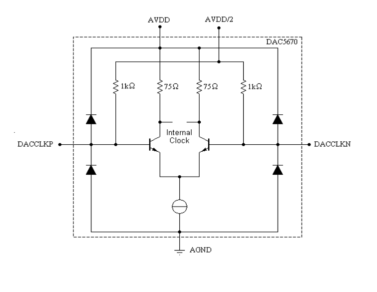 Figure 16. Clock Equivalent Input
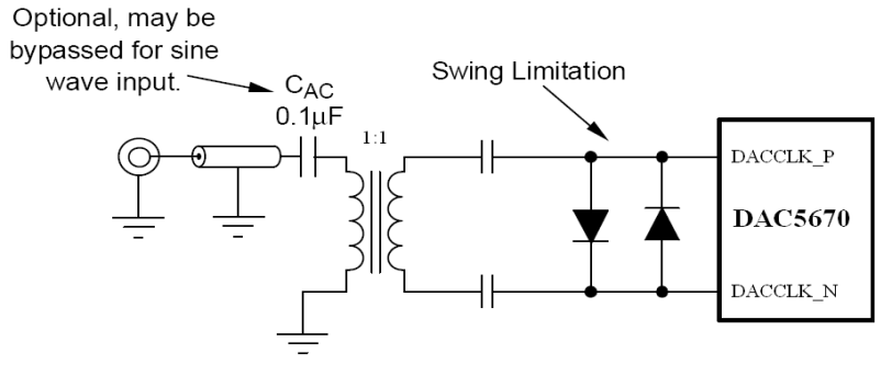 Figure 17. Driving the DAC5670 With a Single-Ended Clock Source Using a Transformer
To obtain the best ac performance, the DAC5670 clock input should be driven with a differential LVPECL or sine wave source as shown in Figure 18 and Figure 19. In this case, set the potential of VTT to the termination voltage required by the driver along with the proper termination resistors (RT). The DAC5670 clock input can also be driven single ended for slower clock rates using TTL/CMOS levels (see Figure 20).
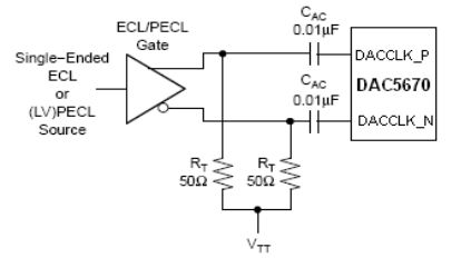 Figure 18. Driving the DAC5670 With a Single-Ended ECL/PECL Clock Source
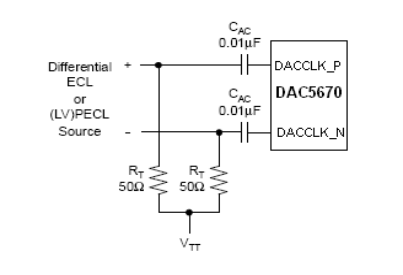 Figure 19. Driving the DAC5670 With a Differential ECL/PECL Clock Source
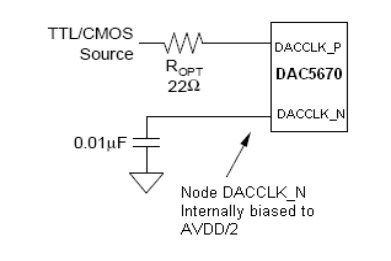 Figure 20. Driving the DAC5670 With a Single-Ended TTL/CMOS Clock Source
8.3.4 DAC Transfer Function
The DAC5670 has a current sink output. The current flow through IOUT_P and IOUT_N is controlled by Dx_P[13:0] and Dx_N[13:0]. For ease of use, this data sheet denotes D[13:0] as the logical bit equivalent of Dx_P[13:0] and its complement Dx_N[13:0]. The DAC5670 supports straight binary coding with D13 as the MSB and D0 as the LSB. Full-scale current flows through IOUTP when all D[13:0] inputs are set high and through IOUTN when all D[13:0] inputs are set low. The relationship between IOUT_P and IOUT_N can be expressed as Equation 1:
IO(FS) is the full-scale output current sink (5 to 30 mA). Because the output stage is a current sink, the current can only flow from AVDD through the load resistors RL into the IOUT_N and IOUT_P pins.
The output current flow in each pin driving a resistive load can be expressed as shown in Figure 21, Equation 2, and Equation 3.
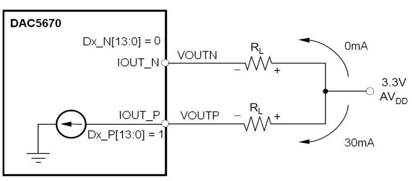 Figure 21. Relationship Between D[13:0], Iout_n and Iout_p
where
- CODE is the decimal representation of the DAC input word
This would translate into single-ended voltages at IOUT_N and IOUT_P, as shown in Equation 4 and Equation 5:
For example, assuming that D[13:0] = 1 and that RL is 50 Ω, the differential voltage between pins IOUT_N and IOUT_P can be expressed as shown in Equation 6 through Equation 8 where IO(FS) = 20 mA:
If D[13:0] = 0, then IOUT_P = 0 mA, IOUT_N = 20 mA, and the differential voltage VDIFF = –1 V.
The output currents and voltages in IOUT_N and IOUT_P are complementary. The voltage, when measured differentially, is doubled compared to measuring each output individually. Take care not to exceed the compliance voltages at the IOUT_N and IOUT_P pins in order to keep signal distortion low.
8.3.5 Reference Operation
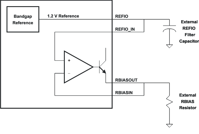 Figure 22. Reference Circuit
The DAC5670 comprises a bandgap reference and control amplifier for biasing the full-scale output current. The full-scale output current is set by applying an external resistor RBIAS to pins RBIASOUT and RBIASIN. The bias current IBIAS through resistor RBIAS is defined by the on-chip bandgap reference voltage and control amplifier. The full-scale output current equals 32× this bias current. The full-scale output current IOUTFS can thus be expressed as:
where
- VREFIO voltage at terminals REFIO and REFIO_IN
The bandgap reference voltage delivers an accurate voltage of 1.2 V. Connect an external REFIO filter capacitor of 0.1 μF externally to the terminals REFIO and REFIO_IN for compensation.
The full-scale output current can be adjusted from 30 to 5 mA by varying external resistor RBIAS.
8.3.6 Analog Current Outputs
Figure 23 is a simplified schematic of the current sink array output with corresponding switches. Differential NPN switches direct the current of each individual NPN current sink to either the positive output node, IOUT_P, or its complementary negative output node, IOUT_N. The input data presented at the DA_P[13:0], DA_N[13:0], DB_P[13:0], and DB_N[13:0] is decoded to control the sw_p(N) and sw_n(N) current switches.
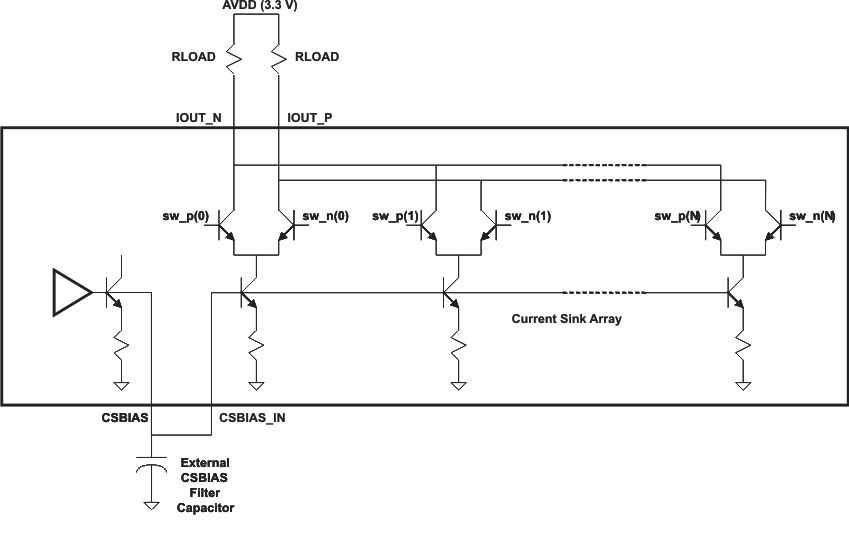 Figure 23. Current Sink Array
The external output resistors, RLOAD, are connected to the positive supply, AVDD.
The DAC5670 can easily be configured to drive a doubly-terminated 50-Ω cable using a properly selected transformer. Figure 24 and Figure 25 show the 1:1 and 4:1 impedance ratio configuration, respectively. These configurations provide maximum rejection of common-mode noise sources and even-order distortion components, thereby doubling the power of the DAC to the output. The center tap on the primary side of the transformer is terminated to AVDD, enabling a dc current flow for both IOUT_N and IOUT_P.
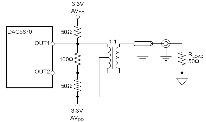 Figure 24. 1:1 Impedance Ratio
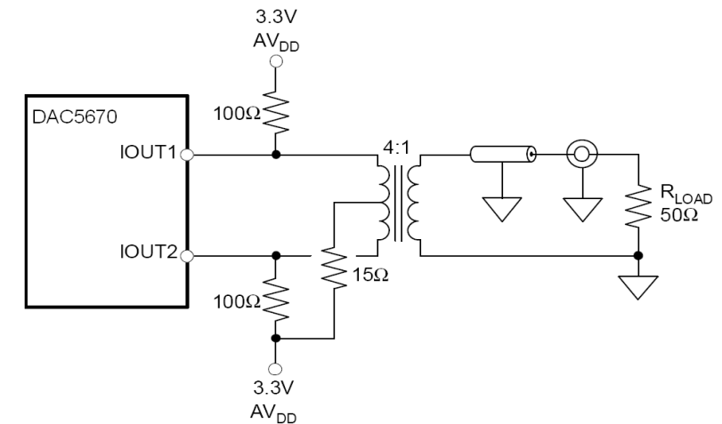 Figure 25. 4:1 Impedance Ratio
8.3.7 Sleep Mode
When the SLEEP pin is asserted (high), the DAC5670 enters a lower-power mode.
8.4 Device Functional Modes
8.4.1 Input Format
The DAC5670 has four input modes selected by the four mutually-exclusive configuration pins: NORMAL, A_ONLY, A_ONLY_INV, and A_ONLY_ZS. Table 1 lists the input modes, input sample rates, maximum DAC sample rate (CLK input), and resulting DAC output sequence for each configuration. For all configurations, the DLYCLK_P/N outputs and DTCLK_P/N inputs are DACCLK_P/N frequency divided by four.
Table 1. DAC5670 Input Formats
| NORMAL | A_ONLY | A_ONLY_INV | A_ONLY_ZS | FinA/Fdac | FinB/Fdac | ƒDAC MAX (MHz) | DLYCLK_P/NAND, DTCLK_P/N FREQ (MHz) | DAC OUTPUT SEQUENCE |
|---|---|---|---|---|---|---|---|---|
| 1 | 0 | 0 | 0 | 1/2 | 1/2 | 2400 | Fdac/4 | A0, B0, A1, B1, A2, B2, . . . |
| 0 | 1 | 0 | 0 | 1/2 | Off | 2400 | Fdac/4 | A0, A0, A1, A1, A2, A2, . . . |
| 0 | 0 | 1 | 0 | 1/2 | Off | 2400 | Fdac/4 | A0, –A0, A1, –A1, A2, –A2, . . |
| 0 | 0 | 0 | 1 | 1/2 | Off | 2400 | Fdac/4 | A0, 0, A1, 0, A2, 0, . . . |