SGLS386F January 2009 – October 2014 DAC5670-SP
PRODUCTION DATA.
- 1 Features
- 2 Applications
- 3 Description
- 4 Revision History
- 5 Description (continued)
- 6 Pin Configuration and Functions
- 7 Specifications
- 8 Detailed Description
- 9 Application and Implementation
- 10Power Supply Recommendations
- 11Layout
- 12Device and Documentation Support
- 13Mechanical, Packaging, and Orderable Information
9 Application and Implementation
NOTE
Information in the following applications sections is not part of the TI component specification, and TI does not warrant its accuracy or completeness. TI’s customers are responsible for determining suitability of components for their purposes. Customers should validate and test their design implementation to confirm system functionality.
9.1 Application Information
The DAC5670 is a 14-bit DAC with max input rate of 2.4 GSPS. The DAC5670 is also suitable to operate at lower sample rates without the use of the DLL for input interface timing.
9.2 Typical Application
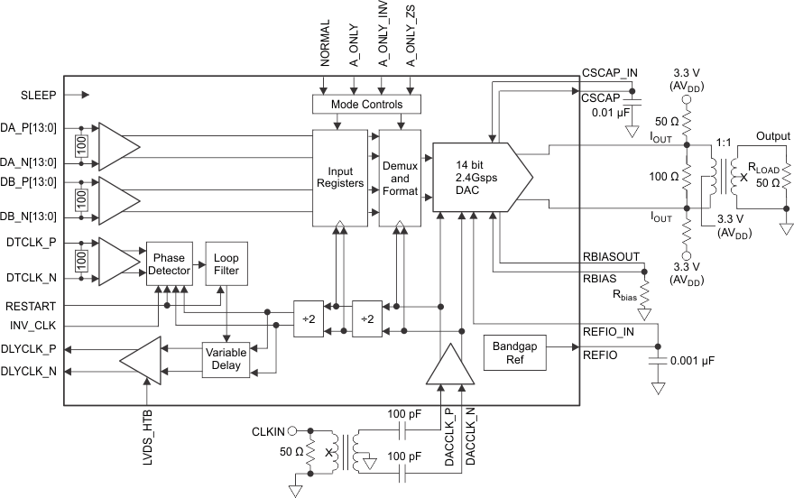 Figure 26. Current Steering DAC5670
9.2.1 Design Requirements
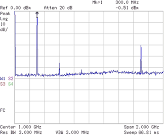
This example uses DACCLK rate of 2 GHz with signal output at 300 MHz.
9.2.2 Detailed Design Procedure
This example is outputting a 300-MHz tone with 2-GHz sample rate. Data is applied to both A and B ports at 1-GHz dual data rate. Full scale IOUT current set to 19.2 mA.
Device settings:
- RESTART low
- LVDS_HTB (pattern generator source dependent)
- INV_CLK as necessary for DLL lock
- SLEEP low
- NORMAL high
- A_ONLY low
- A_ONLY_INV low
- A_ONLY_ZS low
- DA_P[0:13], DA_N[0:13], DB_P[0:13],DB_N[0:13] sourced from pattern generator generating 300-MHz tone with 65536 sample depth
- RBIAS 2 kΩ to GND
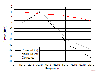
9.2.3 Application Curves