ZHCS597B December 2011 – May 2015 DAC1282
PRODUCTION DATA.
- 1 特性
- 2 应用
- 3 说明
- 4 修订历史记录
- 5 Device Comparison
- 6 Pin Configuration and Functions
- 7 Specifications
-
8 Detailed Description
- 8.1 Overview
- 8.2
Feature Description
- 8.2.1 Signal Output (VOUTP, VOUTN)
- 8.2.2 DAC Modes
- 8.2.3 Reference Voltage (VREF)
- 8.2.4 Output Filter (CAPP, CAPN)
- 8.2.5 Output Switch (SWINP, SWINN, SWOUTP, SWOUTN)
- 8.2.6 Clock Input (CLK)
- 8.2.7 Switch Control/External Digital Input (SW/TD)
- 8.2.8 SYNC
- 8.2.9 RESET/PWDN
- 8.2.10 AVDD, AVSS, and DVDD Power Supplies
- 8.2.11 Step Response
- 8.2.12 Frequency Response
- 8.3 Device Functional Modes
- 8.4 Programming
- 8.5 Register Map
- 9 Application and Implementation
- 10器件和文档支持
- 11机械、封装和可订购信息
8 Detailed Description
8.1 Overview
The DAC1282 is a single-chip, digital-to-analog converter (DAC) that self-generates low-distortion sine-wave and pulse-output signals for the demanding testing requirements of seismic recording equipment. Figure 32 shows the block diagram of the DAC1282.
The DAC1282A device is functionally equivalent to the DAC1282, except that the DAC1282A supports PGA gains of 1/1, 1/4, and 1/16 only. The DAC1282A also relaxes the THD specification of these gains. See the Electrical Characteristics section for more details.
The DAC1282 requires two supply voltages: analog and digital. The analog supply can be single 5 V or bipolar ±2.5 V. The digital supply range is 1.65 V to 3.6V. The output signal common-mode voltage is regulated to
100 mV below the midpoint of the analog power-supply voltage. An internal power-on reset (POR) circuit resets the DAC on power-up.
An SPI™-compatible serial interface is used to access the DAC1282 registers for device configuration and control. The configuration registers can be read back by clocking the data out on the DOUT pin. The DAC1282 voltage output is fully differential and is taken out on the VOUTP/VOUTN pins. The CAPP/CAPN pins connect to external filter capacitors to reduce the output noise.
The reference input voltage sets the DAC1282 full-scale output. The DAC reference voltage is applied between the VREF and AVSS pins. The DAC is optimized to operate with a 5-V reference. The sine-wave generator is programmable by registers to set the sine frequency and amplitude. The frequency range is programmable from 0.4883 Hz to 250 Hz. The output level is controlled by both analog gain (in 6-dB steps), and digital gain (in 0.5-dB steps).
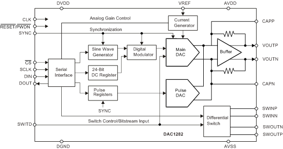 Figure 32. DAC1282 Block Diagram
The digital modulator takes the output from the sine-wave generator or the 24-bit dc register to generate the ones-density bitstream. The bitstream drives the main DAC. Optionally, ones-density data can be input to drive the DAC directly, bypasses the digital signal generator. The main DAC develops a differential output current that is converted to a differential output voltage by an internal current-to-voltage (I/V) amplifier. The output range is set by analog gain that scales the DAC current generator. The output amplifier provides current limit protection.
The dc mode is programmed by a 24-bit register and is used to provide a dc output. The dc mode also has programmable ranges controlled by the analog gain control.
In Pulse mode, a fast-response, 5-bit pulse DAC is used to provide 31 preset dc levels. The levels span over the available output ranges. The pulse DAC is optimized to provide fast response with short output rise times. The pulse DAC is triggered by the SYNC pin for precision control of the pulse time.
The DAC1282 includes a low distortion differential output switch. The output switch can connect the DAC1282 output to sensors for THD and impulse testing. The switch is controlled by either pin or command, thus allowing precise switch timing.
The SYNC input synchronizes the output signal to a known time reference. In sine mode, SYNC resets the sine wave to the zero crossing. In Pulse mode, SYNC selects one of two user-programmed dc levels.
The RESET/PWDN pin powers down the device when low. When RESET/PWDN is released high, the DAC1282 is reset.
The SW/TD input is dual function. In digital data mode, the pin is the ones-density data input. In the other modes, SW/TD controls the opening/closing of the switch.
Figure 33 shows the main details of the main DAC. The main DAC provides the digital-to-analog conversion by filtering the ones-density digital data. In operation, the current generator establishes the range current that is mirrored to a multi-tap, current-steering filter stage. The current generator is controlled by the analog gain control register that scales the weight of the tap currents to one of seven ranges (0 dB to –36 dB).
The current-steering stage switches the tap currents to the positive or negative current summing nodes, as the digital input is sampled. A higher ones-density directs an increasing average current to one node than the other, thus increasing the differential current. The differential current is converted to differential voltage by the internal I/V converter stage. The common-mode current sources balance the current at the amplifier summing node.
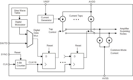 Figure 33. Main DAC Block Diagram
8.2 Feature Description
8.2.1 Signal Output (VOUTP, VOUTN)
As shown in Figure 34, the DAC provides a differential voltage (VDIFF = VOUTP – VOUTN) on pins VOUTP and VOUTN. The output common-mode voltage (VCOM) is regulated to 100 mV below the midpoint of the analog supply (AVDD – AVSS).
Each signal output swings above and below the common-mode voltage. Best performance is realized when the DAC output is used differentially. In power-down mode, the outputs enter a high-impedance, 3-state mode.

NOINDENT:
NOTE: VDIFF = VOUTP – VOUTN = ±2.5 V × Gain (VREF = 5 V).VCOM = –0.1 V (±2.5-V supplies) or 2.4 V (5-V supply).
The DAC output buffer is rated to drive up to a 2-nF capacitive load (maximum) and a 100-Ω resistive load (minimum). However, degradation of THD performance results in resistive loads less than 1 kΩ, as shown in Figure 26
The internal digital modulator generates the signal to drive the DAC. The modulator shapes the in-band noise to high frequency and the frequency-shaped noise is present on the DAC output. However, the high frequency DAC output noise is rejected by the digital filter of the ADC and does not affect system performance.
The DAC sampling update noise is also present on the signal output. The sampling noise does not affect the ADC performance, but when testing the ADC near full-scale input, the noise can cause false indication of the ADC modulator overrange detection. The ADS1282 overrange output signal indication should be ignored when testing at or below the ADC full-scale input.
8.2.2 DAC Modes
The DAC1282 has four operational modes of: sine, dc, pulse, and external digital data input. These modes are programmed by the MODE[1:0] bits in the GANMOD register, as shown in Table 1.
Table 1. DAC Modes
| MODE[1:0] BITS | DAC MODE |
|---|---|
| 00 | Sine |
| 01 | DC |
| 10 | Digital data |
| 11 | Pulse |
8.2.2.1 Sine Mode
In sine mode, the DAC1282 provides a sine-wave output. An internal signal generator develops the sine-wave signal. The M[3:0], N[7:0], and FREQ register bits program the output frequency. The frequency range is programmable from 0.4883 Hz to 250 Hz, as shown in Equation 1.

where
Table 2 lists values of registers M and N for selected output frequencies.
Table 2. Register Output Frequencies
| SIGNAL FREQUENCY (Hz)(1) | M[3:0] REGISTER BITS | N[7:0] REGISTER BITS | FREQ BIT |
|---|---|---|---|
| 0.48828125 | 0000 | 1111 1111 | 1 |
| 0.9765625 | 0000 | 1111 1111 | 0 |
| 1.953125 | 0000 | 0111 1111 | 0 |
| 3.90625 | 0000 | 0011 1111 | 0 |
| 7.8125 | 0000 | 0001 1111 | 0 |
| 15.625 | 0000 | 0000 1111 | 0 |
| 31.25 | 0000 | 0000 0111 | 0 |
| 50 | 0000 | 0000 0100 | 0 |
| 55 | 1010 | 0011 0001 | 0 |
| 60 | 0101 | 0001 1000 | 0 |
| 62.5 | 0000 | 0000 0011 | 0 |
| 100 | 1001 | 0001 1000 | 0 |
| 125 | 0000 | 0000 0001 | 0 |
| 250 | 0000 | 0000 0000 | 0 |
When the M or N registers are updated, the sine wave resets to the zero-crossing point. The sine wave can also be reset to the zero-crossing point by taking the SYNC pin high; see the SYNC section.
The amplitude of the sine-wave output is determined by analog and digital gains. The analog gain increments are 6 dB, from 0 dB to –36 dB, and are programmed by the GAIN[2:0] register bits. Table 3 lists the analog gains.
Table 3. Analog Gain
| ANALOG GAIN (V/V)(1) | ANALOG GAIN (dB)(3) | DIFFERENTIAL RANGE (V)(2) | GAIN[2:0] REGISTER BITS |
|---|---|---|---|
| 1/1 | 0 | ±2.5 | 000 |
| 1/2 | –6 | ±1.25 | 001 |
| 1/4 | –12 | ±0.625 | 010 |
| 1/8 | –18 | ±0.312 | 011 |
| 1/16 | –24 | ±0.156 | 100 |
| 1/32 | –30 | ±0.078 | 101 |
| 1/64 | –36 | ±0.039 | 110 |
The digital gain resolution is in 0.5-dB increments, from 0 dB to full mute and is programmed by the SINEG[7:0] register bits. Table 4 lists the digital gain setting. Equation 2 is the amplitude setting in sine mode.
Best SNR, for a given signal level, is achieved by reducing the analog gain while maximizing the digital gain.
Table 4. Sine Mode Digital Gain
| SINE MODE DIGITAL GAIN (dB) | SINEG[7:0] REGISTER BITS |
|---|---|
| 0 | 0000 0000 |
| –0.5 | 0000 0001 |
| –1.0 | 0000 0010 |
| — | — |
| –119.5 | 1110 1111 |
| Full mute | 1111 0000 |
| Full mute | 1111 xxxx |
| Full mute | 1111 1111 |
8.2.2.2 DC Mode
The DAC1282 provides a dc output mode with 24-bit available resolution. The output level is determined by the analog gain and the 24-bit dc registers.
The GAIN[2:0] register bits set the analog gain (see Table 3). The DCG[23:0] register bits set the 24-bit level over the selected analog range. Table 5 lists the digital gain settings in dc mode.
Table 5. DC Mode Digital Gain Settings
| DIFFERENTIAL OUTPUT VOLTAGE (V)(1) | DCG[23:0] REGISTER BITS |
|---|---|
| +2.5 x Gain | 7FFFFFh |
| +1.25 x Gain | 3FFFFFh |
| 0 | 0 |
| –1.25 x Gain | C00000h |
| –2.5 x Gain | 800001h |
8.2.2.3 Pulse Mode
In pulse mode, a fast responding, 5-bit pulse DAC is used to generate the output. The pulse DAC is designed to approximate a linear-in-dB output function, allowing the generation of pulse test signals across all ranges. Two registers are used to preset the DAC output. The SYNC pin is used to select one of the two registers. When SYNC is low, the PULSA register value drives the DAC; when SYNC is high, the PULSB register value drives the DAC. The pulse registers can be programmed to yield differential outputs from –2.5 V to +2.5 V. Note that the pulse levels scale with VREF and are independent of the analog gain settings. Table 6 lists the programmable range of the pulse A and pulse B registers.
Table 6. Pulse Register Values
| OUTPUT (V)(1) | PULSA[4:0], PULSB[4:0] | OUTPUT (V)(1) | PULSA[4:0], PULSB[4:0] |
|---|---|---|---|
| +2.50 | 01111 | –0.020 | 11111 |
| +1.88 | 01110 | –0.029 | 11110 |
| +1.25 | 01101 | –0.039 | 11101 |
| +0.938 | 01100 | –0.058 | 11100 |
| +0.625 | 01011 | –0.078 | 11011 |
| +0.469 | 01010 | –0.117 | 11010 |
| +0.312 | 01001 | –0.156 | 11001 |
| +0.234 | 01000 | –0.234 | 11000 |
| +0.156 | 00111 | –0.312 | 10111 |
| +0.117 | 00110 | –0.469 | 10110 |
| +0.078 | 00101 | –0.625 | 10101 |
| +0.058 | 00100 | –0.938 | 10100 |
| +0.039 | 00011 | –1.25 | 10011 |
| +0.029 | 00010 | –1.88 | 10010 |
| +0.020 | 00001 | –2.50 | 10001 |
| 0 | 00000 | ||
Note that when pulse testing the ADC, the ADC digital filter time domain response has characteristic overshoot and ringing. As a result of the ADC filter overshoot, input levels close to ADC full scale may cause clipping of the ADC output code.
8.2.2.4 Digital Data Mode
In digital data mode, the DAC internal signal generator is bypassed and the DAC is driven instead by applying a bitstream input. Arbitrary DAC output waveforms can be generated by application of custom digital data patterns. The data format in this mode is ones-density modulated input at CLK/16 data rate (256 kHz). The input is applied to the SW/TD input pin. The DAC1282 output in digital data mode is defined in Equation 3.
where
The DAC1282 filters the digital data (bitstream) input providing a voltage output proportional to the bitstream ones-density. The GAIN[2:0] register sets the analog gain in 6-dB steps, from 0 dB to –36 dB (1/1 to 1/64); see the SYNC section for the external timing requirements. Table 7 lists several values of the external bitstream input.
Table 7. External Bitstream Input
| ONES-DENSITY BITSTREAM (%) | VOUTP – VOUTN (V)(1) |
|---|---|
| 25 | –2.5 × Gain |
| 37.5 | –1.25 × Gain |
| 50 | 0 |
| 62.5 | +1.25 × Gain |
| 75 | +2.5 × Gain |
8.2.3 Reference Voltage (VREF)
The DAC1282 requires an external reference for operation. Although reference voltage as low as 2.5 V can be used, best SNR is achieved with a 5-V reference. The reference input is defined as the voltage difference between VREF and AVSS (that is, VREF = VREF – AVSS). The DAC1282 output scales with VREF; consequently, reference noise or drift appears on the DAC output. Excessive reference noise may lead to degraded SNR. A low-drift and low-noise reference is recommended.
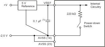
Connect the external reference ground pin directly to the AVSS pins using a star connector to AVSS pin 14. Star connection minimizes the possibility of power-supply crosstalk. Also, connect a 0.1-µF capacitor close to the VREF and AVSS terminals to reduce noise susceptibility. Figure 35 shows the reference connection. The reference input impedance is 220 kΩ. In power-down the switch is off, resulting in very high input impedance. For single-supply applications, connect AVSS to a clean analog ground point.
NOINDENT:
Recommended bypass capacitor.8.2.4 Output Filter (CAPP, CAPN)
The CAPP and CAPN pins are the connections for two external capacitors, one capacitor connects to CAPP and VOUTP and the other capacitor connects to CAPN and VOUTN. The capacitors are required to filter the DAC sampling noise. The capacitor values are 1 nF; capacitors with low voltage coefficients should be used (C0G ceramic or film).
As seen in Figure 36, the external capacitors form an analog low-pass filter with the internal feedback resistors. After step changes to the data in the sine, dc, and digital data modes, the settling of the DAC and the analog filter is 100-µs typical, as shown in Figure 46. In pulse mode, the filter is internally disabled, yielding shorter settling time.
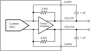 Figure 36. Output Filter
8.2.5 Output Switch (SWINP, SWINN, SWOUTP, SWOUTN)
The DAC1282 has an integrated output switch. The switch can be used to route the DAC output signal to a sensor for pulse, THD, and common-mode testing. The switch has low on-resistance and matched elements to minimize signal distortion. The switch input voltage range extends to the analog power supply.
The switch is controlled by three register bits, SW[2:0], and is also controlled by the SW/TD input pin. The switch integrates break-before-make operation when the register or the SW/TD input control is changed. The SW/TD input can be used to force the switch open for precise timing control of sensor impulse testing; see the Switch Control/DAC Data Input (SW/TD) section. Figure 37 and Table 8 describe the switch operation.
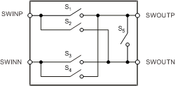 Figure 37. DAC1282 Signal Switch
Note that when the DAC is in power-down mode, the switch is forced open.
As shown in Figure 29, the switch on-resistance varies with the switch signal level. When the switch is used to route the signal and a resistive load is connected to the switch output, the switch on-resistance variations interact with the load resistance and cause the THD to degrade. Figure 27 illustrates the dependence of THD versus switch load resistance. The dependence of THD data was taken with a full-scale signal.
Table 8. Switch Connections
| DESCRIPTION | PIN CONNECTIONS | SWITCHES CLOSED | SW[2:0] REGISTER BITS |
|---|---|---|---|
| Open (default) | Open | None | 000 |
| Differential | SWINP to SWOUTP and SWINN to SWOUTN | S1, S3 | 001 |
| Differential reverse | SWINP to SWOUTN and SWINN to SWOUTP | S2, S4 | 010 |
| Common-mode positive | SWINP to SWOUTP and SWOUTN | S1, S2 | 011 |
| Common-mode negative | SWINN to SWOUTP and SWOUTN | S3, S4 | 100 |
| Single-ended positive | SWINP to SWOUTP | S1 | 101 |
| Single-ended negative | SWINN to SWOUTN | S3 | 110 |
| Output short | SWOUTP to SWOUTN | S5 | 111 |
8.2.6 Clock Input (CLK)
The CLK pin is the master clock input to the DAC1282, nominally 4.096 MHz. As with any high-performance data converter, a high-quality clock source is essential. A crystal oscillator or low-jitter PLL clock source is recommended. Make sure to avoid ringing on the input by keeping the trace short and source-terminating (typically 50 Ω). See the CLK specifications shown in Figure 38 and Table 9.
 Figure 38. CLK Timing Requirements
Table 9. Requirements for Figure 38
| SYMBOL | DESCRIPTION | MIN | MAX | UNIT |
|---|---|---|---|---|
| tCLK | CLK period | 235 | 1000 | ns |
| tCPWH, L | CLK pulse width high or low | 95 | 900 | ns |
8.2.7 Switch Control/External Digital Input (SW/TD)
SW/TD is a multi-function digital input pin. The SW/TD function depends on the mode of operation.
8.2.7.1 SW Function
In sine, dc, and pulse mode, SW/TD controls the output switch. When SW/TD is low, all switches are forced open, overriding the switch register setting (SW[2:0]). When SW/TD is high, the switch is transparent to the value of register setting. In power-down mode, the switch is forced open.
8.2.7.2 TD Function
In digital input mode, SW/TD is the signal input used to drive the DAC. The data input are modulated by ones-density and are clocked in by the master clock (CLK). When the ones-density is 75% (that is, on average, three out of four bits are '1'), the differential output voltage is at the positive maximum value. When the ones-density is 25% (that is, on average, three out of four bits are '0'), the differential output voltage is at the negative maximum value. When the ones-density is 50% (on average, an equal number of '0's and '1's), the differential output is zero.
SW/TD is sampled by the DAC1282 at the rate of CLK/16. Therefore, the sampling can have ±8 CLK periods of uncertainty. SYNC can be used to eliminate the uncertainty by synchronizing the phase of SW/TD to the desired CLK cycle. Synchronizing the digital input results in a consistent phase of the output signal; see the SYNC section.
The output range is set by the analog gain bits, GAIN[2:0]; see Table 3. Equation 3 describes the DAC output versus the bitstream input ones-density. Make sure to avoid ringing on the input by keeping the trace short. In some cases, source-terminating resistors may be necessary (20 Ω to 50 Ω).
8.2.8 SYNC
SYNC is a digital input used to synchronize the DAC1282 output.
In the digital data mode, the DAC input is a ones-density bitstream. In this mode, the SYNC pin synchronizes the sampling of SW/TD digital data to the desired master clock cycle (CLK). When SYNC is low or high, the DAC operates normally. When SYNC is taken from low to high, the DAC output is reset to zero and the sample instant of SW/TD is reset to the eighth rising CLK edge that follows. The SW/TD is then regularly sampled on subsequent 16 CLK intervals. After synchronization, the DAC output is not settled and achieves full settling 400 CLK periods later, as shown in Figure 39.
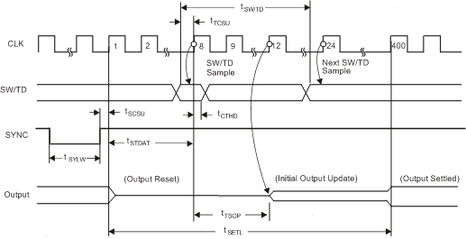 Figure 39. Digital Data Mode Synchronization
Table 10. Timing Characteristics for Figure 39(1)
| SYMBOL | DESCRIPTION | MIN | TYP | UNIT |
|---|---|---|---|---|
| tSCSU | SYNC high to CLK high setup time | 30 | ns | |
| tTCSU | SW/TD to CLK high setup time | 30 | ns | |
| tCTHD | CLK high to SW/TD hold time | 10 | ns | |
| tSYLW | SYNC low pulse width | 2 | tCLK | |
| tSTDAT | CLK high after SYNC high to SW/TD sample time | 8 | tCLK | |
| tTSOP | SW/TD sample to output update | 4 | tCLK | |
| tSW/TD | SW/TD period | 16 | tCLK | |
| tSETL | SYNC high to fully-settled output | 400 | tCLK |
In sine mode, the SYNC rising edge resets the DAC output to differential 0 V (sine-wave zero-crossing point). When SYNC is high or low, the output is unaffected. When SYNC is taken from low to high, the output resets on the following CLK rising edge. SYNC must be pulsed low for a minimum of 2 CLK cycles. The SYNC input can be applied simultaneous to the DAC and the ADS1282 (ADC in pulse-sync mode).
To synchronize the DAC, observe SYNC to the CLK timing requirements shown in Figure 40. That is, the SYNC rising edge should be applied before the set-up time or after the hold time specifications. If the SYNC timing requirement is not met, the DAC may synchronize with one clock cycle timing error.
 Figure 40. Sine Mode Synchronization
Table 11. Timing Characteristics for Figure 40(1)
| SYMBOL | DESCRIPTION | MIN | UNIT |
|---|---|---|---|
| tSYLO | SYNC pulse width low | 2 | tCLK |
| tSCSU | SYNC rising edge to CLK rising edge setup time | 30 | ns |
| tCSHD | CLK rising edge to SYNC rising edge hold time | 40 | ns |
In pulse mode, the SYNC pin selects one of two pre-programmed pulse levels. The pulse levels are programmable from +2.5 V to –2.5 V in approximately 3-dB steps by pulse level registers PULSA and PULSB. When SYNC is low, the value of the PULSA register drives the DAC; when SYNC is high, the value of the PULSB register is the code of the DAC, as shown in Figure 41. When the SYNC pin is changed, the DAC output updates immediately to the new code.
 Figure 41. Sync Operation in Pulse Mode
8.2.9 RESET/PWDN
The RESET/PWDN is a digital input used to power-down and reset the DAC1282. To power-down the DAC, take the pin low. In power-down mode, the power consumption is reduced to a device leakage level (see the Electrical Characteristics table). The signal output and digital pin DOUT enters 3-state and the output switch is driven off. Note that the digital inputs must remain defined as either logic low or logic high; do not float the inputs. Disable the CLK input to minimize leakage. To exit the power-down state, take the pin high. The DAC1282 is reset after power-down mode is exited.
The DAC1282 is reset by taking the RESET/PWDN pin low for a minimum of two fCLK cycles and is then taken back high. The DAC1282 is held in reset for 2 fCLK cycles; after this time, DAC communications may begin, as shown in Figure 42 and Table 12.
 Figure 42. DAC RESET/PWDN
Table 12. Timing Characteristics for Figure 42
| SYMBOL | DESCRIPTION | MIN | MAX | UNIT |
|---|---|---|---|---|
| tRSLO | PWDN/RESET pulse width low for power-down | 500 | ns | |
| tRSTM | PWDN/RESET high to begin operation | 500 | ns |
8.2.10 AVDD, AVSS, and DVDD Power Supplies
The DAC1282 has two power supplies: analog and digital. The analog supply (AVDD, AVSS) is 5 V and can either be single 5 V or dual (±2.5 V). The analog supply should be clean and free from noise and ripple. The DAC1282 regulates the output common-mode voltage to 0.1 V below the mid-point of the analog supply. Because the analog supply pins draw signal-dependent current and AVSS (pin 14) is internally shared with the reference input low, trace resistance between AVSS (pin 14) and the AVSS power supply should be minimized or degraded performance may result. Therefore, connect the external reference ground terminal close to the device AVSS terminal using a star connection. This configuration helps to minimize power-supply coupling to the reference input.
DVDD is the digital supply used to power both the internal digital and the device I/O pins. The allowable range of DVDD is 1.65 V to 3.6 V.
The power supplies can be sequenced on or off in any order, but the analog or digital inputs should never exceed AVDD or AVSS, or DVDD, respectively. In such an event, the internal ESD protection diodes may begin to conduct. The input current must always be limited as specified in the Absolute Maximum Ratings table.
At power-on, when the latter of DVDD exceeds approximately 1.3 V, or the difference of AVDD – AVSS exceeds approximately 1.4 V, an internal power-on reset (POR) occurs. During POR, the device is held in a reset condition for a period of 216 fCLK periods as shown in Figure 43. During this time, the DAC1282 output is held at 0 V, differential. SPI communications are not possible during this time. After the reset time elapses, the default settings are loaded: 31.25 Hz, 28 mVRMS amplitude, and output switch off. SPI communications can then be started.
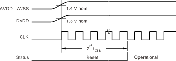 Figure 43. Power-On Sequence
8.2.10.1 Power Consumption
The power consumed by the DAC1282 depends on the analog gain. Table 13 shows the DAC power consumption.
Table 13. Power Consumption
| ANALOG GAIN | POWER (mW)(1) |
|---|---|
| 1/1 | 38 |
| 1/2 | 28 |
| 1/4 | 23 |
| 1/8 | 21 |
| 1/16 | 20 |
| 1/32 | 20 |
| 1/64 | 20 |
8.2.10.2 Offset and Gain Error
The DAC1282 features a low offset error ( ±7/Gain + 50 ppm FS typical) and low gain error (0.1 % typical). Offset and gain drift are also very low for the DAC1282. Drift is calculated using the box calculation method of Equation 4:
where
Gain match is the gain error of Gain = 1/1 relative to all analog gains.
8.2.10.3 Signal-to-Noise Ratio (SNR)
The DAC1282 achieves excellent signal-to-noise ratio (SNR) performance. The SNR data are obtained using the DAC circuit of Figure 50 and data captured by the ADS1282.
SNR is measured with a signal level of –0.5 dBFS and a 31.25-Hz test frequency, then taking the fast fourier transform (FFT) of 4096 data points from the ADS1282, using complementing gains. The noise power is calculated over the bandwidth of 413 Hz (1-ms sample period). The dc, fundamental, and harmonic bins are removed to calculate the SNR. The SNR measurement represents the combination of the ADS1282 SNR and the SNR of the DAC1282.
8.2.10.4 DC Noise
DC noise data are obtained using the DAC circuit of Figure 50 with data captured by the ADS1282. The noise is measured in dc mode with the output voltage set to 0 V differential. The ADC gain is set to the complement of the DAC gain for each output range. The noise is the standard deviation of 4096-point ADC acquisition record (RMS noise, referred-to-output).
8.2.10.5 Total Harmonic Distortion (THD)
The DAC1282 achieves excellent THD performance. The THD data are obtained using the DAC circuit of Figure 50 and captured by the ADS1282. The ADC gain is set to the complement of the DAC gain for each output range.
THD is measured with a –0.5-dBFS output signal level and a 31.25-Hz test frequency, then taking the FFT of the 4096-point ADC acquisition record. The ADC data points are increased to 16,384 for gains of 1/16, 1/32, and 1/64 for improved rendition of harmonics as a result of the higher noise floor. The THD measurement represents the combination of the ADS1282 THD and the DAC1282 THD.
8.2.11 Step Response
The step response of the DAC depends on the mode. In pulse mode, the DAC disables the external analog filter formed by capacitors CAPP, CAPN. Disabling the analog filter in conjunction with the fast response pulse DAC results in noticeably faster rise time and shorter settling time. Note that additional filter components in the signal path may also affect the response time.
Figure 44 shows the pulse mode step response after the SYNC pin transition. Figure 45 shows the pulse mode detail settling to 0.1% of final value after the SYNC pin transition.
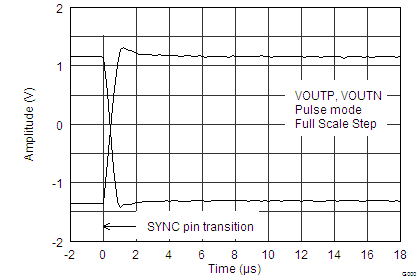
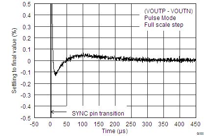
Figure 46 shows the step response time of the dc mode. The step response of sine and digital data mode have similar settling times. Note that additional filter components in the signal path may also affect the response time.
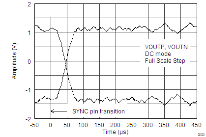 Figure 46. DC-Mode Step Response
8.2.12 Frequency Response
The DAC internal signal generator is capable of output signal frequencies from 0.489 Hz to 250 Hz. Frequencies outside of this range are also possible by driving the DAC directly with an external digital input (bitstream). However, the DAC low-pass filters the digital input and results in a sinx/x frequency response. The –3 dB signal bandwidth of the DAC filter is 8.2 kHz. Figure 47 illustrates the DAC1282 frequency response. Note that high-order noise-shaped digital inputs may limit the useable frequency range as a result of rising noise.
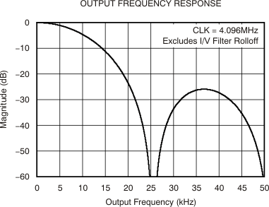 Figure 47. DAC Frequency Response
8.3 Device Functional Modes
8.3.1 Serial Interface
Configuration of the DAC is by an SPI-compatible serial interface consisting of four signals: CS, SCLK, DIN, and DOUT; or the interface can consist of three signals in which case CS may be tied low. Tying CS low permanently selects the device and DOUT remains a driven output. The interface is used to read and write registers and also is used to send a DAC reset command.
8.3.1.1 Serial Communications
DAC1282 communication occurs by clocking register data into the device (on DIN) and reading back register data (on DOUT). The SCLK input is used to clock data into and out of the device. Data are input on the serial clock (SCLK) rising edge and output on the SCLK falling edge. The communication protocol is half-duplex (that is, data are transmitted to and from the device one direction at a time).
Communications to the device occur on 8-bit boundaries. If an unintentional SCLK transition should occur (such as is possible from a noise spike), the DAC1282 command decoder can be out-of-sync and the serial port may not respond properly. The serial port may reset in one of the following ways:
- Take CS high to reset the interface
- Hold SCLK inactive (low state) for 218 fCLK cycles to automatically reset the interface (see the SPI Timeout section)
- Take RESET/PWDN low then back high to reset the device and the interface
- Cycle the power supplies for a power-on reset (POR)
8.3.1.2 Chip Select (CS)
CS (chip select) selects the DAC1282 for communication. To select the device, pull CS low. CS must remain low for the duration of the command sequence. When CS is taken high, the serial interface is reset, input commands are ignored, and DOUT enters a high-impedance state.
8.3.1.3 Serial Clock (SCLK)
The serial clock (SCLK) is a Schmitt-triggered input used to clock data into and out of the DAC1282. SCLK can be idled high or low. If SCLK is idled low, the SPI timeout feature is active. If SCLK is idled high, the SPI timeout feature is disabled.
Despite the built-in Schmitt-trigger, keep SCLK as clean as possible to prevent glitches from accidently shifting the data. Series-terminated printed circuit board (PCB) traces often help to reduce ringing and overshoot (series termination resistance is approximately 20 Ω to 50 Ω). If SCLK is held low for 218 fCLK periods, the serial interface is reset. The timeout feature can be used to automatically recover the SPI port in the event of a noise glitch. Avoid starting new commands after this time interval to prevent an unexpected serial port reset at the next command instant.
8.3.1.4 Data Input (DIN)
DIN is the data input pin used to send data to the DAC. The DAC1282 latches DIN input data on the rising edge of SCLK.
8.3.1.5 Data Output (DOUT)
DOUT is the data output pin used to read register data out of the DAC. The data are shifted out on the falling edge of SCLK. DOUT enters a 3-state when CS is high.
8.3.2 SPI Timeout
The DAC has an SPI timeout feature that can be used to recover the SPI port if a possible noise pulse should occur. The noise pulse may lead to a false SCLK detection that can render the DAC serial port unresponsive. The port is recovered by taking CS high but, in applications where CS is tied low, holding SCLK low for 218 CLK cycles resets the SPI port automatically. When SCLK is low, the SPI port resets on every 218 CLK cycle interval. Holding SCLK high disables the automatic SPI reset.
8.4 Programming
8.4.1 Commands
The commands summarized in Table 14 control and configure the DAC1282. The register read and register write commands are two-byte command arguments plus additional data bytes while the reset command is a one-byte command. The DAC1282 serial port chip select (CS) can be taken high or held low between commands but must remain low for the entire command operation.
Table 14. Command Definitions
| COMMAND | TYPE | DESCRIPTION | FIRST OPCODE BYTE | SECOND OPCODE BYTE |
|---|---|---|---|---|
| RREG | Register | Read nnnn register(s) at address rrrr(1) | 0010 rrrr | 0000 nnnn |
| WREG | Register | Write nnnn register(s) at address rrrr | 0100 rrrr | 0000 nnnn |
| RESET | Control | Reset the device | 0000 011x (06 or 07h) | — |
8.4.1.1 RREG: Read From Registers
Description: These two opcode bytes read register data. The register read operation is a two-byte opcode input followed by one or more bytes of register data as the output. The first byte of the command is the opcode and the register address combined. The second byte of the command specifies the number of registers to read (minus 1) in a block. Register data are output following the command input. Note that for multiple register read operations, the register address pointer does not wrap when the last register is exceeded.
First opcode byte: 0010 rrrr, where rrrr is the starting address register address to be read.
Second opcode byte: 0000 nnnn, where nnnn is the number of registers to read – 1.
Following bytes: Register data output in MSB-first format. The 16th SCLK falling edge of the opcode clocks out the MSB of the register data.

(Opcode 1 = 0010 0000, Opcode 2 = 0000 0001)
8.4.1.2 WREG: Write To Registers
Description: These two opcode bytes write register data. The register write operation is a two-byte opcode followed by one or more bytes of register data. The first byte of the command is the write opcode and the register address combined. The second byte of the command specifies the number of registers to write (minus 1) in a single sequence. The following bytes are the register data bytes. Note that for multiple register write operations, the register address pointer does not wrap when the last register is exceeded.
First opcode byte: 0010 rrrr, where rrrr is the starting address register address to be written.
Second opcode byte: 0000 nnnn, where nnnn is the number of registers to write – 1.
Following bytes: Register data input in MSB-first format.

(Opcode 1 = 0100 0000, Opcode 2 = 0000 0001)
8.4.1.3 RESET: Device Reset
Description: This command resets the DAC. The registers are set to power-on default the value; see the RESET/PWDN section.
8.5 Register Map
DAC1282 operation is controlled through a set of 8-bit registers. Collectively, the registers contain all the information needed to configure the DAC, such as output frequency and amplitude, output pulse levels, etc. Table 15 shows the register map.
The default state of the device at power-up, after the RESET pin is taken high or after a RESET command is as follows:
Sine mode, frequency = 31.25 Hz, –36-dB output range, 0-dB digital attenuation
Switch state: open
Table 15. Register Map
| ADDRESS | REGISTER | DEFAULT | BIT 7 | BIT 6 | BIT 5 | BIT 4 | BIT 3 | BIT 2 | BIT 1 | BIT 0 |
|---|---|---|---|---|---|---|---|---|---|---|
| 0 | GANMOD | xxx11000 | ID2 | ID1 | ID0 | GAIN2 | GAIN1 | GAIN0 | MODE1 | MODE0 |
| 1 | SING | 00000000 | SINEG7 | SINEG6 | SINEG5 | SINEG4 | SINEG3 | SINEG2 | SINEG1 | SINEG0 |
| 2 | SWM | 00000000 | FREQ | SW2 | SW1 | SW0 | M3 | M2 | M1 | M0 |
| 3 | N | 00000111 | N7 | N6 | N5 | N4 | N3 | N2 | N1 | N0 |
| 4 | DCG0 | 00000000 | DCG7 | DCG6 | DCG5 | DCG4 | DCG3 | DCG2 | DCG1 | DCG0 |
| 5 | DCG1 | 00000000 | DCG15 | DCG14 | DCG13 | DCG12 | DCG11 | DCG10 | DCG9 | DCG8 |
| 6 | DCG2 | 00000000 | DCG23 | DCG22 | DCG21 | DCG20 | DCG19 | DCG18 | DCG17 | DCG16 |
| 7 | PULSA | 00000000 | 0 | 0 | 0 | PULSA4 | PULSA3 | PULSA2 | PULSA1 | PULSA0 |
| 8 | PULSB | 00000000 | 0 | 0 | 0 | PULSB4 | PULSB3 | PULSB2 | PULSB1 | PULSB0 |
8.5.1 Register Descriptions
Table 1. GANMOD: Range and Mode Register 0 (address = 0h)
| 7 | 6 | 5 | 4 | 3 | 2 | 1 | 0 |
| ID2 | ID1 | ID0 | GAIN2 | GAIN1 | GAIN0 | MODE1 | MODE0 |
| Bits[7:5] | ID[2:0]: Factory-programmed identification bits (read-only) | ||||
| These bits may change at any time without notification. | |||||
| Bits[4:2] | GAIN[2:0]: Analog gain (output range) | ||||
| These bits set the analog gain in the sine, dc, and bitstream modes. The output amplitude is the combination of the selected range and the digital gain. Sine mode digital gain is programmed by the SINEG register; dc mode digital gain are the DCG0, DCG1, and DCG2 registers. Pulse mode levels are exclusively controlled by the PULSA and PULSB registers. Note that the DAC1282A supports analog gains of 1/1, 1/4, and 1/16 only. | |||||
| GAIN[2:0] | DEVICE GAIN | OUTPUT RANGE (V)(1) | |||
| 000 | 0 dB | 1/1 V/V | ±2.5 | ||
| 001 (DAC1282 only) | –6 dB | 1/2 V/V | ±1.25 | ||
| 010 | –12 dB | 1/4 V/V | ±0.625 | ||
| 011 (DAC1282 only) | –18 dB | 1/8 V/V | ±0.312 | ||
| 100 | –24 dB | 1/16 V/V | ±0.156 | ||
| 101 (DAC1282 only) | –30 dB | 1/32 V/V | ±0.078 | ||
| 110 (DAC1282 only, default)(2) | –36 dB | 1/64 V/V | ±0.039 | ||
| Bits[1:0] | MODE[1:0]: Mode control bits | ||||
| The mode bits set the mode of operation. When the mode bits are changed, the internal signal generator block is reset. | |||||
| 00 = Sine mode (default) 01 = DC mode 10 = Digital data mode 11 = Pulse mode |
|||||
Table 2. SINEG: Sine Mode Digital Gain Register (address = 01h)
| 7 | 6 | 5 | 4 | 3 | 2 | 1 | 0 |
| SINEG7 | SINEG6 | SINEG5 | SINEG4 | SINEG3 | SINEG2 | SINEG1 | SINEG0 |
| Bits[7:0] | SINEG[7:0]: Sine mode digital gain |
| This register byte sets the sine mode digital gain from 0 dB to –119.5 dB and to full mute, in 0.5-dB steps. The sine mode digital gain can be expressed as: –DGAIN[7:0]/2 (dB) and are listed in Table 16. |
Table 16. Sine Mode Digital Gain
| SINEG[7:0] REGISTER | SINE MODE DIGITAL GAIN (dB) |
|---|---|
| 0000 0000 (default) | 0.0 |
| 0000 0001 | –0.5 |
| 0000 0010 | –1.0 |
| … | … |
| 1110 1111 | –119.5 |
| 1111 0000 | Full mute |
| … | Full mute |
| 1111 1111 | Full mute |
Table 3. SWM: Switch, Output Frequency 'M', And Range Bit Register (address = 02h)
| 7 | 6 | 5 | 4 | 3 | 2 | 1 | 0 |
| FREQ | SW2 | SW1 | SW0 | M3 | M2 | M1 | M0 |
| Bit 7 | FREQ: Frequency | ||
| This bit sets the sine mode output frequency range; see Equation 1. | |||
| Bits[6:4] | SW[2:0]: Switch control bits | ||
| These bits control the switch settings when the SW/TD input is high. When SW/TD is low, the register is ignored and the switch is forced open. In digital input mode, the switch is controlled only by the register. | |||
| SW[2:0] | SWITCH DESCRIPTION | TERMINAL CONNECTIONS | |
| 000 | Open (default) | All switches open | |
| 001 | Differential | SWINP to SWOUTP and SWINN to SWOUTN | |
| 010 | Differential reverse | SWINP to SWOUTN and SWINN to SWOUTP | |
| 011 | Common-mode positive | SWINP to SWOUTP and SWINP to SWOUTN | |
| 100 | Common-mode negative | SWINN to SWOUTP and SWINN to SWOUTN | |
| 101 | Single-ended positive | SWINP to SWOUTP only | |
| 110 | Single-ended negative | SWINN to SWOUTN only | |
| 111 | Short | SWOUTP to SWOUTN | |
| Bits[3:0] | M[3:0]: Sine mode frequency, M bits | ||
| These bits control the sine-mode output frequency. The output frequency is given in Equation 1. | |||
Table 4. N: Sine Frequency N Register (address = 03h)
| 7 | 6 | 5 | 4 | 3 | 2 | 1 | 0 |
| N7 | N6 | N5 | N4 | N3 | N2 | N1 | N0 |
| Bits[7:0] | N[7:0]: N register |
| These bits control the output frequency; see Equation 1. |
Table 5. DCG0: DC Mode Digital Gain Byte 0, Least Significant Byte (address = 04h)
| 7 | 6 | 5 | 4 | 3 | 2 | 1 | 0 |
| DCG7 | DCG6 | DCG5 | DCG4 | DCG3 | DCG2 | DCG1 | DCG0 |
Table 6. DCG1: DC Mode Digital Gain Byte 1, Mid Byte (address = 05h)
| 7 | 6 | 5 | 4 | 3 | 2 | 1 | 0 |
| DCG15 | DCG14 | DCG13 | DCG12 | DCG11 | DCG10 | DCG9 | DCG8 |
Table 7. DCG2: DC Mode Digital Gain Byte 2, Most Significant Byte (address = 06h)
| 7 | 6 | 5 | 4 | 3 | 2 | 1 | 0 |
| DCG23 | DCG22 | DCG21 | DCG20 | DCG19 | DCG18 | DCG17 | DCG16 |
| Bits[7:0] | DCG[23:0]: DC mode digital gain setting | |
| The DCG0, DCG1, and DCG2 register bytes set the digital gain in dc mode; see Table 5. | ||
Table 8. PULSA: Pulse Level A Byte (address = 07h)
| 7 | 6 | 5 | 4 | 3 | 2 | 1 | 0 |
| 0 | 0 | 0 | PULSA4 | PULSA3 | PULSA2 | PULSA1 | PULSA0 |
| Bits[7:5] | Reserved |
| Always write '0'. | |
| Bits[4:0] | PULSA[4:0]: Pulse level A bits |
| These bits create pulse level A. (Selected output when SYNC is low.) | |
| The PULSA and PULSB registers set two independent levels that can be used to provide pulse output. The SYNC pin selects either level PULSA or level PULSB as the DAC output. The pulse amplitude resolution is programmable in discrete steps, as shown in Table 6. Note that the pulse level value is independent of the RANGE[2:0] setting. |
Table 9. PULSB: Pulse Level B Byte (address = 08h)
| 7 | 6 | 5 | 4 | 3 | 2 | 1 | 0 |
| 0 | 0 | 0 | PULSB4 | PULSB3 | PULSB2 | PULSB1 | PULSB0 |
| Bits[7:5] | Reserved |
| Always write '0'. | |
| Bits[4:0] | PULSB[4:0]: Pulse level B bits |
| These bits create pulse level B. | |
| The PULSA and PULSB registers set two independent levels that can be used to provide pulse output. The SYNC pin selects either level PULSA or level PULSB as the DAC output. The pulse amplitude resolution is programmable in discrete steps; see Table 6. Note that the pulse level value is independent of the RANGE[2:0] setting. |